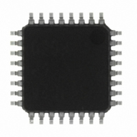
M37544G2AGP#U0 Renesas Electronics America, M37544G2AGP#U0 Datasheet - Page 74

M37544G2AGP#U0
Manufacturer Part Number
M37544G2AGP#U0
Description
IC 740 MCU OTP 8K 32LQFP
Manufacturer
Renesas Electronics America
Series
740/38000r
Specifications of M37544G2AGP#U0
Core Processor
740
Core Size
8-Bit
Speed
8MHz
Connectivity
SIO, UART/USART
Peripherals
WDT
Number Of I /o
25
Program Memory Size
8KB (8K x 8)
Program Memory Type
QzROM
Ram Size
256 x 8
Voltage - Supply (vcc/vdd)
4 V ~ 5.5 V
Data Converters
A/D 6x8b
Oscillator Type
Internal
Operating Temperature
-20°C ~ 85°C
Package / Case
32-LQFP
Lead Free Status / RoHS Status
Lead free / RoHS Compliant
Eeprom Size
-
Available stocks
Company
Part Number
Manufacturer
Quantity
Price
REJ03B0108-0103
page 72 of 72
7544 Group (QzROM version)
Notes on Oscillation Stop Detection Circuit
1. Oscillation stop detection status bit is initialized by the following
(1) External reset
(2) Write “0” data to the ceramic or RC oscillation stop detection
2. The oscillation stop detection circuit is not included in the emu-
Note on Power Source Voltage
When the power source voltage value of a microcomputer is less
than the value which is indicated as the recommended operating
conditions, the microcomputer does not operate normally and may
perform unstable operation.
In a system where the power source voltage drops slowly when
the power source voltage drops or the power supply is turned off,
reset a microcomputer when the supply voltage is less than the
recommended operating conditions and design a system not to
cause errors to the system by this unstable operation.
NOTES ON HARDWARE
1. Handling of Power Source Pin
In order to avoid a latch-up occurrence, connect a capacitor suit-
able for high frequencies as bypass capacitor between power
source pin (Vcc pin) and GND pin (Vss pin). Besides, connect the
capacitor to as close as possible. For bypass capacitor which
should not be located too far from the pins to be connected, a ce-
ramic capacitor of 0.01 µF to 0.1 µF is recommended.
2. Handling of CNVss Pin
The CNVss pin is connected to the internal memory circuit block
by a low-ohmic resistance, since it has the multiplexed function to
be a programmable power source pin (V
To improve the noise reduction, connect a track between CNVss
pin and Vss pin with 1 to 10 kΩ resistance.
NOTES ON QzROM
Product shipped in blank
As for the product shipped in blank, Renesas does not perform the
writing test to user ROM area after the assembly process though
the QzROM writing test is performed enough before the assembly
process. Therefore, a writing error of approx.0.1 % may occur.
Moreover, please note the contact of cables and foreign bodies on
a socket, etc. because a writing environment may cause some
writing errors.
operation.
function active bit.
lator MCU “M37544RSS”.
Rev.1.03
Mar 31, 2009
PP
pin) as well.
Precautions Regarding Overvoltage
Make sure that voltage exceeding the V
plied to other pins. In particular, ensure that the state indicated by
bold lines in Figure below does not occur for CNV
power source pin for QzROM) during power-on or power-off.
Otherwise the contents of QzROM could be rewritten.
Fig. 7 Timing Diagram (bold-lined periods are applicable)
Notes on QzROM Writing Orders
When ordering the QzROM product shipped after writing, submit
the mask file (extension: .msk) which is made by the mask file
converter MM.
• Be sure to set the ROM option data* setup when making the
• Set “FF
* ROM option data: mask option noted in MM
DATA REQUIRED FOR QzROM WRITING
ORDERS
The following are necessary when ordering a QzROM product
shipped after writing:
1. QzROM Writing Confirmation Form*
2. Mark Specification Form*
3. ROM data...........Mask file
* For the QzROM writing confirmation form and the mark specifi-
cation form, refer to the “Renesas Technology Corp.” Homepage
(http://www.renesas.com/homepage.jsp).
Note that we cannot deal with special font marking (customer's
trademark etc.) in QzROM microcomputer.
mask file by using the mask file converter MM.. The ROM code
protect is specified according to the ROM option data* in the
mask file which is submitted at ordering. Note that the mask file
which has nothing at the ROM option data* or has the data other
than “00
gardless of the presence or absence of a protect. When data
other than “FF
mitted again.
CNV
“L” input
V
CC
SS
pin voltage
pin voltage
(1) Input voltage to other MCU pins rises before V
(2) Input voltage to other MCU pins falls after V
Note: The internal circuitry is unstable when V
16
16
” to the ROM code protect address in ROM data re-
” and “FF
specification of 1.8V (shaded portion), so particular care should be exercised
regarding overvoltage.
16
” is set, we may ask that the ROM data be sub-
1.8V
16
” can not be accepted.
CC
CC
is below the minimum voltage
CC
CC
pin voltage.
pin voltage.
pin voltage is not ap-
1.8V
SS
pin (V
PP


