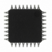
M37544G2AGP#U0 Renesas Electronics America, M37544G2AGP#U0 Datasheet - Page 47

M37544G2AGP#U0
Manufacturer Part Number
M37544G2AGP#U0
Description
IC 740 MCU OTP 8K 32LQFP
Manufacturer
Renesas Electronics America
Series
740/38000r
Specifications of M37544G2AGP#U0
Core Processor
740
Core Size
8-Bit
Speed
8MHz
Connectivity
SIO, UART/USART
Peripherals
WDT
Number Of I /o
25
Program Memory Size
8KB (8K x 8)
Program Memory Type
QzROM
Ram Size
256 x 8
Voltage - Supply (vcc/vdd)
4 V ~ 5.5 V
Data Converters
A/D 6x8b
Oscillator Type
Internal
Operating Temperature
-20°C ~ 85°C
Package / Case
32-LQFP
Lead Free Status / RoHS Status
Lead free / RoHS Compliant
Eeprom Size
-
Available stocks
Company
Part Number
Manufacturer
Quantity
Price
REJ03B0108-0103
page 45 of 72
7544 Group (QzROM version)
Table 9 Pin description (QzROM writing mode)
QzROM Writing Mode
In the QzROM writing mode, the user ROM area can be rewritten
while the microcomputer is mounted on-board by using a serial
programmer which is applicable for this microcomputer.
Table 9 lists the pin description (QzROM writing mode) and Fig. 50
and Fig. 51 show the pin connections.
Refer to Fig. 52 and Fig. 53 for example of a connection with a se-
rial programmer.
Contact the manufacturer of your serial programmer for serial pro-
grammer . Refer to the user's manual of your serial programmer
for details on how to use it.
V
____________
RESET
X
X
V
P0
P1
P2
P3
CNV
P1
P1
P1
CC
IN
OUT
REF
1
0
3
0
0
2
0
–P0
–P1
–P2
–P3
, V
SS
Pin
SS
7
4
5
4
, P3
7
Power source
Reset input
Clock input
Clock output
Analog reference voltage
I/O port
V
ESDA input/output
ESCLK input
ESPGMB input
PP
Rev.1.03
input
Name
Mar 31, 2009
Output
Input
Input
Input
Input
Input
Input
Input
I/O
I/O
I/O
•Apply 1.8 to 5.5V to V
•Reset input pin for active “L”. Reset occurs when RESET pin is hold at
an “L” level for 16 cycles or more of X
•Set the same termination as the single-chip mode.
•Input the reference voltage of A/D converter to V
•Input “H” or “L” level signal or leave the pin open.
•QzROM programmable power source pin.
•Serial data I/O pin.
•Serial clock input pin.
•Read/program pulse input pin.
CC
, and 0V to V
Function
IN
SS
.
.
REF
____________
.


