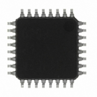
M37544G2AGP#U0 Renesas Electronics America, M37544G2AGP#U0 Datasheet - Page 63

M37544G2AGP#U0
Manufacturer Part Number
M37544G2AGP#U0
Description
IC 740 MCU OTP 8K 32LQFP
Manufacturer
Renesas Electronics America
Series
740/38000r
Specifications of M37544G2AGP#U0
Core Processor
740
Core Size
8-Bit
Speed
8MHz
Connectivity
SIO, UART/USART
Peripherals
WDT
Number Of I /o
25
Program Memory Size
8KB (8K x 8)
Program Memory Type
QzROM
Ram Size
256 x 8
Voltage - Supply (vcc/vdd)
4 V ~ 5.5 V
Data Converters
A/D 6x8b
Oscillator Type
Internal
Operating Temperature
-20°C ~ 85°C
Package / Case
32-LQFP
Lead Free Status / RoHS Status
Lead free / RoHS Compliant
Eeprom Size
-
Available stocks
Company
Part Number
Manufacturer
Quantity
Price
REJ03B0108-0103
page 61 of 72
7544 Group (QzROM version)
Note: As for AD translation accuracy, on the following operating conditions, accuracy may become low.
Timing Requirements
Table 16 Timing requirements (V
Note: In this time, bit 6 of the serial I/O control register (address 001A
A/D Converter Characteristics
Table 15 A/D Converter characteristics (V
t
t
t
t
t
t
t
t
t
t
t
t
t
t
t
—
ABS
t
R
I
I
W
C
WH
WL
C
WH
WL
C
WH
WL
C
WH
WL
su
h
Symbol
CONV
VREF
I(AD)
(S
(X
(CNTR
(CNTR
(S
LADDER
(RESET)
(RxD–S
______
(X
(CNTR
(CNTR
(S
(X
(CNTR
(CNTR
(S
(1) Since the analog circuit inside a microcomputer becomes sensitive to noise when V
(2) When V
CLK
When bit 6 of the serial I/O control register is “0” (clock asynchronous serial I/O is selected), the rating values are divided by 4.
IN
CLK
Symbol
IN
CLK
IN
CLK
)
)
–RxD)
accuracy may become low rather than the case where V
the time of room temperature. The use beyond V
is assumed to be.
)
)
0
1
)
)
)
)
0
1
CLK
0
1
)
)
)
)
Resolution
Absolute accuracy
(quantification error excluded)
Conversion time
Ladder resistor
Reference power source
input current
A/D port input current
)
REF
voltage is less than [ 3.0V ], the accuracy at the time of low temperature may become extremely low compared with
Rev.1.03
Reset input “L” pulse width
External clock input cycle time
External clock input “H” pulse width
External clock input “L” pulse width
CNTR
CNTR
CNTR
CNTR
CNTR
CNTR
Serial I/O clock input cycle time (Note)
Serial I/O clock input “H” pulse width (Note)
Serial I/O clock input “L” pulse width (Note)
Serial I/O input set up time
Serial I/O input hold time
0
0
0
1
1
1
Parameter
, INT
, INT
input cycle time
input cycle time
input “H” pulse width
input “L” pulse width
CC
0
0
Mar 31, 2009
, INT
, INT
= 1.8 to 5.5 V, V
1
1
, input “H” pulse width
, input “L” pulse width
CC
= 2.7 to 5.5 V, V
Parameter
SS
= 0 V, Ta = –20 to 85 °C, unless otherwise noted)
REF
Ta = –20 to 85 °C, Vcc = V
V
V
=3.0V is recommended in the system the use by the side of low temperature
16
REF
REF
) is set to “1” (clock synchronous serial I/O is selected).
SS
REF
= 5.0 V
= 3.0 V
= 0 V, Ta = –20 to 85 °C, unless otherwise noted)
Test conditions
voltage and Vcc voltage are set up to the same value..
REF
REF
Min.
2000
Min.
50
30
125
200
800
800
800
370
370
220
100
voltage is set up lower than Vcc voltage,
50
50
80
80
2
Limits
Typ.
135
Limits
37
80
Typ.
Max.
109
200
120
5.0
±3
8
Max.
tc(X
Unit
LSB
Bits
kΩ
µA
µA
Unit
µs
ns
ns
ns
ns
ns
ns
ns
ns
ns
ns
ns
ns
ns
ns
IN
)


