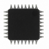
M37544G2AGP#U0 Renesas Electronics America, M37544G2AGP#U0 Datasheet - Page 27

M37544G2AGP#U0
Manufacturer Part Number
M37544G2AGP#U0
Description
IC 740 MCU OTP 8K 32LQFP
Manufacturer
Renesas Electronics America
Series
740/38000r
Specifications of M37544G2AGP#U0
Core Processor
740
Core Size
8-Bit
Speed
8MHz
Connectivity
SIO, UART/USART
Peripherals
WDT
Number Of I /o
25
Program Memory Size
8KB (8K x 8)
Program Memory Type
QzROM
Ram Size
256 x 8
Voltage - Supply (vcc/vdd)
4 V ~ 5.5 V
Data Converters
A/D 6x8b
Oscillator Type
Internal
Operating Temperature
-20°C ~ 85°C
Package / Case
32-LQFP
Lead Free Status / RoHS Status
Lead free / RoHS Compliant
Eeprom Size
-
Available stocks
Company
Part Number
Manufacturer
Quantity
Price
REJ03B0108-0103
page 25 of 72
7544 Group (QzROM version)
Key Input Interrupt (Key-On Wake-Up)
A key-on wake-up interrupt request is generated by applying “L”
level to any pin of port P0 that has been set to input mode.
In other words, it is generated when the AND of input level goes
from “1” to “0”. An example of using a key input interrupt is shown
in Fig. 22, where an interrupt request is generated by pressing
one of the keys provided as an active-low key matrix which uses
ports P0
Fig. 22 Connection example when using key input interrupt and port P0 block diagram
0
to P0
3
as input ports.
Rev.1.03
P0
P0
P0
P0
P0
P0
P0
P0
7
6
5
4
output
output
output
output
3
2
1
0
input
input
input
input
Mar 31, 2009
Port PXx
“L” level output
Port P0
selection bit
*
*
*
*
*
*
*
*
0
PULL register
bit 3 = “0”
PULL register
bit 3 = “0”
PULL register
bit 3 = “0”
PULL register
bit 3 = “0”
PULL register
bit 2 = “1”
PULL register
bit 2 = “1”
PULL register
bit 1 = “1”
PULL register
bit 0 = “1”
key-on wakeup
**
**
**
**
**
**
**
**
Port P0
latch
Port P0
latch
Port P0
latch
Port P0
latch
Port P0
latch
Port P0
latch
Port P0
latch
Port P0
latch
7
6
5
4
3
2
1
0
Port P0
Direction register = “1”
Port P0
Direction register = “1”
Port P0
Direction register = “1”
Port P0
Direction register = “1”
Port P0
Direction register = “0”
Port P0
Direction register = “0”
Port P0
Direction register = “0”
Port P0
Direction register = “0”
7
6
5
4
3
2
1
0
Falling edge
detection
Falling edge
detection
Falling edge
detection
Falling edge
detection
Falling edge
detection
Falling edge
detection
Falling edge
detection
Falling edge
detection
** CMOS output buffer
* P-channel transistor for pull-up
Key input interrupt request
Port P0
Input read circuit


