M30833FJFP#U3 Renesas Electronics America, M30833FJFP#U3 Datasheet - Page 11
M30833FJFP#U3
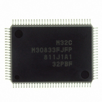
Manufacturer Part Number
M30833FJFP#U3
Description
IC M32C/83 MCU FLASH 100QFP
Manufacturer
Renesas Electronics America
Series
M16C™ M32C/80r
Datasheets
1.M3087BFLGPU3.pdf
(364 pages)
2.M30833FJGPU3.pdf
(96 pages)
3.M30833FJGPU3.pdf
(529 pages)
Specifications of M30833FJFP#U3
Core Processor
M32C/80
Core Size
16/32-Bit
Speed
32MHz
Connectivity
CAN, I²C, IEBus, SIO, UART/USART
Peripherals
DMA, WDT
Number Of I /o
85
Program Memory Size
512KB (512K x 8)
Program Memory Type
FLASH
Ram Size
31K x 8
Voltage - Supply (vcc/vdd)
3 V ~ 5.5 V
Data Converters
A/D 26x10b; D/A 2x8b
Oscillator Type
Internal
Operating Temperature
-40°C ~ 85°C
Package / Case
100-QFP
For Use With
R0K330879S001BE - KIT DEV RSK M32C/87R0K330879S000BE - KIT DEV RSK M32C/87
Lead Free Status / RoHS Status
Lead free / RoHS Compliant
Eeprom Size
-
Available stocks
Company
Part Number
Manufacturer
Quantity
Price


17. A/D Converter ______________________________ 224
16.2 Clock Asynchronous Serial I/O (UART) Mode ................................................... 188
16.3 Special Mode 1 (I
16.4 Special Mode 2 ..................................................................................................... 204
16.5 Special Mode 3 (GCI Mode) ................................................................................. 210
16.6 Special Mode 4 (IE Mode) .................................................................................... 214
16.7 Special Mode 5 (SIM Mode) ................................................................................. 218
17.1 Mode Description ................................................................................................. 234
17.2 Function ................................................................................................................ 236
16.2.1 Bit Rate .......................................................................................................... 192
16.2.2 Selecting LSB First or MSB First ................................................................. 193
16.2.3 Serial Data Logic Inverse ............................................................................. 193
16.2.4 TxD and RxD I/O Polarity Inverse ................................................................ 194
16.3.1 Detecting Start Condition and Stop Condition .......................................... 200
16.3.2 Start Condition or Stop Condition Output .................................................. 201
16.3.3 Arbitration ...................................................................................................... 202
16.3.4 Transfer Clock ............................................................................................... 202
16.3.5 SDA Output .................................................................................................... 202
16.3.6 SDA Input ....................................................................................................... 203
16.3.7 ACK, NACK .................................................................................................... 203
16.3.8 Transmit and Receive Reset ........................................................................ 203
16.4.1 SSi Input Pin Function (i=0 to 4) .................................................................. 207
16.4.2 Clock Phase Setting Function ..................................................................... 208
16.7.1 Parity Error Signal ........................................................................................ 222
16.7.2 Format ............................................................................................................ 223
17.1.1 One-shot Mode .............................................................................................. 234
17.1.2 Repeat Mode .................................................................................................. 234
17.1.3 Single Sweep Mode ...................................................................................... 235
17.1.4 Repeat Sweep Mode 0 .................................................................................. 235
17.1.5 Repeat Sweep Mode 1 .................................................................................. 236
17.2.1 Resolution Select Function .......................................................................... 236
17.2.2 Sample and Hold ........................................................................................... 236
17.2.3 Trigger Select Function ................................................................................ 236
17.2.4 Two-Circuit Simultaneous Start (Software Trigger) ................................... 237
17.2.5 Pin Input Replacement Function ................................................................. 237
17.2.6 Extended Analog Input Pins ........................................................................ 238
17.2.7 External Operation Amplifier (Op-Amp) Connection Mode....................... 238
17.2.8 Power Consumption Reducing Function ................................................... 239
17.2.9 Analog Input Pin and External Sensor Equivalent Circuit ........................ 239
______
2
C Mode) .................................................................................. 195
A-5
Related parts for M30833FJFP#U3
Image
Part Number
Description
Manufacturer
Datasheet
Request
R

Part Number:
Description:
KIT STARTER FOR M16C/29
Manufacturer:
Renesas Electronics America
Datasheet:

Part Number:
Description:
KIT STARTER FOR R8C/2D
Manufacturer:
Renesas Electronics America
Datasheet:

Part Number:
Description:
R0K33062P STARTER KIT
Manufacturer:
Renesas Electronics America
Datasheet:

Part Number:
Description:
KIT STARTER FOR R8C/23 E8A
Manufacturer:
Renesas Electronics America
Datasheet:

Part Number:
Description:
KIT STARTER FOR R8C/25
Manufacturer:
Renesas Electronics America
Datasheet:

Part Number:
Description:
KIT STARTER H8S2456 SHARPE DSPLY
Manufacturer:
Renesas Electronics America
Datasheet:

Part Number:
Description:
KIT STARTER FOR R8C38C
Manufacturer:
Renesas Electronics America
Datasheet:

Part Number:
Description:
KIT STARTER FOR R8C35C
Manufacturer:
Renesas Electronics America
Datasheet:

Part Number:
Description:
KIT STARTER FOR R8CL3AC+LCD APPS
Manufacturer:
Renesas Electronics America
Datasheet:
Part Number:
Description:
KIT STARTER FOR RX610
Manufacturer:
Renesas Electronics America
Datasheet:

Part Number:
Description:
KIT STARTER FOR R32C/118
Manufacturer:
Renesas Electronics America
Datasheet:

Part Number:
Description:
KIT DEV RSK-R8C/26-29
Manufacturer:
Renesas Electronics America
Datasheet:

Part Number:
Description:
KIT STARTER FOR SH7124
Manufacturer:
Renesas Electronics America
Datasheet:

Part Number:
Description:
KIT STARTER FOR H8SX/1622
Manufacturer:
Renesas Electronics America
Datasheet:

Part Number:
Description:
KIT DEV FOR SH7203
Manufacturer:
Renesas Electronics America
Datasheet: