M30833FJFP#U3 Renesas Electronics America, M30833FJFP#U3 Datasheet - Page 330
M30833FJFP#U3
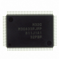
Manufacturer Part Number
M30833FJFP#U3
Description
IC M32C/83 MCU FLASH 100QFP
Manufacturer
Renesas Electronics America
Series
M16C™ M32C/80r
Datasheets
1.M3087BFLGPU3.pdf
(364 pages)
2.M30833FJGPU3.pdf
(96 pages)
3.M30833FJGPU3.pdf
(529 pages)
Specifications of M30833FJFP#U3
Core Processor
M32C/80
Core Size
16/32-Bit
Speed
32MHz
Connectivity
CAN, I²C, IEBus, SIO, UART/USART
Peripherals
DMA, WDT
Number Of I /o
85
Program Memory Size
512KB (512K x 8)
Program Memory Type
FLASH
Ram Size
31K x 8
Voltage - Supply (vcc/vdd)
3 V ~ 5.5 V
Data Converters
A/D 26x10b; D/A 2x8b
Oscillator Type
Internal
Operating Temperature
-40°C ~ 85°C
Package / Case
100-QFP
For Use With
R0K330879S001BE - KIT DEV RSK M32C/87R0K330879S000BE - KIT DEV RSK M32C/87
Lead Free Status / RoHS Status
Lead free / RoHS Compliant
Eeprom Size
-
Available stocks
Company
Part Number
Manufacturer
Quantity
Price


R
R
M
e
E
3
. v
J
2
Table 21.29 Registers to be Used and Settings
0
GiBCR0
GiBCR1
GiPOCR0
GiPOCR1
GiPO0
GiPO1
GiFS
GiFE
GiMR
GiEMR
GiCR
GiETC
GiERC
GiIRF
GiCMP0,
GiCMP1
GiCMP2
GiCMP3
GiMSK0,
GiMSK1
GiTCRC
GiRCRC
GiTO
GiRI
GiRB
GiTB
i = 0,1
1
C
9
3 .
B
Register
8 /
0
1
3
0
3
J
G
4
a
0 -
n
o r
3 .
1
u
, 1
3
p
1
2
(
M
0
0
3
BCK1 to BCK0
DIV4 to DIV0
IT
7 to 0
7 to 0
7 to 0
15 to 0
15 to 0
FSC1 to FSC0
IFE1 to IFE0
GMD1 to GMD0
CKDIR
UFORM
IRS
7 to 0
TI
TXEPT
RI
TE
RE
SOF
TCRCE
ABTE
TBSF0, TBSF1
CMP2E to CMP0E Select whether received data is compared or not
CMP3E
RCRCE
RSHTE
RBSF0, RBSF1
BSERR, ABT
IRF3 to IRF0
7 to 0
7 to 0
7 to 0
7 to 0
15 to 0
15 to 0
7 to 0
7 to 0
7 to 0
7 to 0
6
2
C
8 /
Page 305
Bit
, 3
M
3
2
C
f o
8 /
4
3
8
Select count source
Select divide ratio of count source
Select the base timer interrupt
Set to "0001 0010
Set to "0000 0000
Set to "0000 0000
Set bit rate
Set the timing of the rising edge of the transfer clock.
Timing of the falling edge (high-level signal ("H") width of the transfer clock) is
fixed.
Setting value of GiPO1
Set to "00
Set to "11
Set to "11
Set to "0"
Set to "0"
Select how the transmit interrupt is generated
Set to "1111 0110
Transmit buffer empty flag
Transmit register empty flag
Receive complete flag
Transmit enable bit
Receive enable bit
Set to "0"
Select whether the transmit CRC is used or not
Set to "0"
Transmit bit stuffing
Set to "1"
Select whether receive CRC is used or not
Set to "1" to use it in the receiver
Receive bit stuffing
Set to "0"
Select how an interrupt is generated
Write "FE
Data to be compared
Write "7E
Write "01
Transmit CRC calculation result can be read
Receive CRC calculation result can be read
Data, which is output from a transmit data generation circuit, can be read
Set data input to a receive data generation circuit
Received data is stored
For transmission : write data to be transmitted
For reception
) T
8
16
16
16
2
2
2
"
"
"
" to abort processing
"
" to abort processing
: received data for comparison is stored
2
2
2
2
"
"
"
"
21. Intelligent I/O (Group 0, 1 Communication Function)
Setting value of GiPO0 .
Function
Related parts for M30833FJFP#U3
Image
Part Number
Description
Manufacturer
Datasheet
Request
R

Part Number:
Description:
KIT STARTER FOR M16C/29
Manufacturer:
Renesas Electronics America
Datasheet:

Part Number:
Description:
KIT STARTER FOR R8C/2D
Manufacturer:
Renesas Electronics America
Datasheet:

Part Number:
Description:
R0K33062P STARTER KIT
Manufacturer:
Renesas Electronics America
Datasheet:

Part Number:
Description:
KIT STARTER FOR R8C/23 E8A
Manufacturer:
Renesas Electronics America
Datasheet:

Part Number:
Description:
KIT STARTER FOR R8C/25
Manufacturer:
Renesas Electronics America
Datasheet:

Part Number:
Description:
KIT STARTER H8S2456 SHARPE DSPLY
Manufacturer:
Renesas Electronics America
Datasheet:

Part Number:
Description:
KIT STARTER FOR R8C38C
Manufacturer:
Renesas Electronics America
Datasheet:

Part Number:
Description:
KIT STARTER FOR R8C35C
Manufacturer:
Renesas Electronics America
Datasheet:

Part Number:
Description:
KIT STARTER FOR R8CL3AC+LCD APPS
Manufacturer:
Renesas Electronics America
Datasheet:
Part Number:
Description:
KIT STARTER FOR RX610
Manufacturer:
Renesas Electronics America
Datasheet:

Part Number:
Description:
KIT STARTER FOR R32C/118
Manufacturer:
Renesas Electronics America
Datasheet:

Part Number:
Description:
KIT DEV RSK-R8C/26-29
Manufacturer:
Renesas Electronics America
Datasheet:

Part Number:
Description:
KIT STARTER FOR SH7124
Manufacturer:
Renesas Electronics America
Datasheet:

Part Number:
Description:
KIT STARTER FOR H8SX/1622
Manufacturer:
Renesas Electronics America
Datasheet:

Part Number:
Description:
KIT DEV FOR SH7203
Manufacturer:
Renesas Electronics America
Datasheet: