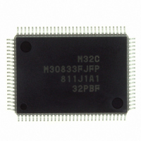
M30833FJFP#U3 Renesas Electronics America, M30833FJFP#U3 Datasheet - Page 41

M30833FJFP#U3
Manufacturer Part Number
M30833FJFP#U3
Description
IC M32C/83 MCU FLASH 100QFP
Manufacturer
Renesas Electronics America
Series
M16C™ M32C/80r
Datasheets
1.M3087BFLGPU3.pdf
(364 pages)
2.M30833FJGPU3.pdf
(96 pages)
3.M30833FJGPU3.pdf
(529 pages)
Specifications of M30833FJFP#U3
Core Processor
M32C/80
Core Size
16/32-Bit
Speed
32MHz
Connectivity
CAN, I²C, IEBus, SIO, UART/USART
Peripherals
DMA, WDT
Number Of I /o
85
Program Memory Size
512KB (512K x 8)
Program Memory Type
FLASH
Ram Size
31K x 8
Voltage - Supply (vcc/vdd)
3 V ~ 5.5 V
Data Converters
A/D 26x10b; D/A 2x8b
Oscillator Type
Internal
Operating Temperature
-40°C ~ 85°C
Package / Case
100-QFP
For Use With
R0K330879S001BE - KIT DEV RSK M32C/87R0K330879S000BE - KIT DEV RSK M32C/87
Lead Free Status / RoHS Status
Lead free / RoHS Compliant
Eeprom Size
-
Available stocks
Company
Part Number
Manufacturer
Quantity
Price
- Current page: 41 of 529
- Download datasheet (5Mb)
R
R
M
e
E
3
. v
I : Input
NOTE:
J
2
0
Table 1.6 Pin Description (100-Pin and 144-Pin Packages) (Continued)
Serial I/O
Special Function
Reference
Voltage Input
A/D Converter
D/A Converter
Intelligent I/O
CAN
Classsfication
C
1
9
3 .
B
1. Available in the 144-pin package only.
8 /
0
1
3
0
3
J
G
4
a
o r
0 -
n
3 .
O : Output
u
1
, 1
3
p
1
(
2
M
0
_______
STxD0 to
STxD4
SRxD0 to
SRxD4
SS0 to SS4
V
AN
AN0
AN2
AN15
___________
AD
ANEX0
ANEX1
DA0, DA1
INPC0
INPC0
INPC0
INPC1
INPC1
INPC1
OUTC0
OUTC0
OUTC0
OUTC1
OUTC1
OUTC1
OUTC2
OUTC2
OUTC2
OUTC3
OUTC3
to OUTC3
ISCLK0 to ISCLK2
ISCLK3
ISRXD0 to ISRXD3
ISTXD0 to ISTXD3
BE0
BE0
IE
IE
CAN
CAN
0
3
6
2
REF
OUT
Symbol
IN
C
OUT,
0
TRG
IN,
0
0
0
0
1
0
4
5
0
3
7
0
3
7
0
1
8 /
to AN
(1)
(1)
(1)
, OUTC3
IN
OUT
to AN0
to AN2
to AN15
to INPC0
to INPC1
to OUTC0
to
to OUTC1
to
to OUTC2
to
to OUTC3
7
BE1
3
7
6
7
BE1
(1)
Page 16
, 3
(1)
(1)
_______
to
to
(1)
I/O : Input and output
OUT
IN
M
3
7
7
7
7
2
2
2
2
2
2
3
I/O Type
2
C
I/O
I/O
f o
O
O
O
O
O
O
O
8 /
I
I
I
I
I
I
I
I
I
I
I
4
3
8
) T
8
Outputs serial data when slave mode is selected
Inputs serial data when slave mode is selected
Input pins to control serial I/O special function
Applies reference voltage to the A/D converter and D/A converter
Analog input pins for the A/D converter
Input pin for an external A/D trigger
Extended analog input pin for the A/D converter and output pin in external
op-amp connection mode
Extended analog input pin for the A/D converter
Output pin for the D/A converter
Input pins for the time measurement function
Output pins for the waveform generating function
(OUTC2
Inputs and outputs the clock for the intelligent I/O communication function
Inputs data for the intelligent I/O communication function
Outputs data for the intelligent I/O communication function
Inputs data for the intelligent I/O communication function
Outputs data for the intelligent I/O communication function
Inputs data for the intelligent I/O communication function
Outputs data for the intelligent I/O communication function
Input pin for the CAN communication function
Output pin for the CAN communication function
0
and OUTC2
2
assigned to P7
0
and P7
Function
1
are pins for the N-channel open drain output.)
1. Overview
Related parts for M30833FJFP#U3
Image
Part Number
Description
Manufacturer
Datasheet
Request
R

Part Number:
Description:
KIT STARTER FOR M16C/29
Manufacturer:
Renesas Electronics America
Datasheet:

Part Number:
Description:
KIT STARTER FOR R8C/2D
Manufacturer:
Renesas Electronics America
Datasheet:

Part Number:
Description:
R0K33062P STARTER KIT
Manufacturer:
Renesas Electronics America
Datasheet:

Part Number:
Description:
KIT STARTER FOR R8C/23 E8A
Manufacturer:
Renesas Electronics America
Datasheet:

Part Number:
Description:
KIT STARTER FOR R8C/25
Manufacturer:
Renesas Electronics America
Datasheet:

Part Number:
Description:
KIT STARTER H8S2456 SHARPE DSPLY
Manufacturer:
Renesas Electronics America
Datasheet:

Part Number:
Description:
KIT STARTER FOR R8C38C
Manufacturer:
Renesas Electronics America
Datasheet:

Part Number:
Description:
KIT STARTER FOR R8C35C
Manufacturer:
Renesas Electronics America
Datasheet:

Part Number:
Description:
KIT STARTER FOR R8CL3AC+LCD APPS
Manufacturer:
Renesas Electronics America
Datasheet:

Part Number:
Description:
KIT STARTER FOR RX610
Manufacturer:
Renesas Electronics America
Datasheet:

Part Number:
Description:
KIT STARTER FOR R32C/118
Manufacturer:
Renesas Electronics America
Datasheet:

Part Number:
Description:
KIT DEV RSK-R8C/26-29
Manufacturer:
Renesas Electronics America
Datasheet:

Part Number:
Description:
KIT STARTER FOR SH7124
Manufacturer:
Renesas Electronics America
Datasheet:

Part Number:
Description:
KIT STARTER FOR H8SX/1622
Manufacturer:
Renesas Electronics America
Datasheet:

Part Number:
Description:
KIT DEV FOR SH7203
Manufacturer:
Renesas Electronics America
Datasheet:


