M30833FJFP#U3 Renesas Electronics America, M30833FJFP#U3 Datasheet - Page 368
M30833FJFP#U3
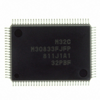
Manufacturer Part Number
M30833FJFP#U3
Description
IC M32C/83 MCU FLASH 100QFP
Manufacturer
Renesas Electronics America
Series
M16C™ M32C/80r
Datasheets
1.M3087BFLGPU3.pdf
(364 pages)
2.M30833FJGPU3.pdf
(96 pages)
3.M30833FJGPU3.pdf
(529 pages)
Specifications of M30833FJFP#U3
Core Processor
M32C/80
Core Size
16/32-Bit
Speed
32MHz
Connectivity
CAN, I²C, IEBus, SIO, UART/USART
Peripherals
DMA, WDT
Number Of I /o
85
Program Memory Size
512KB (512K x 8)
Program Memory Type
FLASH
Ram Size
31K x 8
Voltage - Supply (vcc/vdd)
3 V ~ 5.5 V
Data Converters
A/D 26x10b; D/A 2x8b
Oscillator Type
Internal
Operating Temperature
-40°C ~ 85°C
Package / Case
100-QFP
For Use With
R0K330879S001BE - KIT DEV RSK M32C/87R0K330879S000BE - KIT DEV RSK M32C/87
Lead Free Status / RoHS Status
Lead free / RoHS Compliant
Eeprom Size
-
Available stocks
Company
Part Number
Manufacturer
Quantity
Price


R
R
M
e
E
3
. v
J
Figure 22.17 C0GMR0, C0LMAR0 and C0LMBR0 Registers
2
0
22.1.15 CAN0 Global Mask Register, CAN0 Local Mask Register A and CAN0 Local Mask
C
1
9
3 .
B
8 /
0
1
3
The C0GMRj, C0LMARj and C0LMBRj registers are used for acceptance filtering.
The C0GMRj register determines whether the IDs in the message slots 0 to 13 are verified. The
C0LMARj register determines whether the ID in the message slot 14 is verified. The C0LMBRj register
determines whether the ID in the message slot 15 is verified.
0
3
J
G
NOTES:
4
• When bits in these registers are set to "0", each ID bit, standard ID 0 to 1 bit and extended ID0 to
• When bits in these registers are set to "1", corresponding ID bits are compared with received IDs
a
o r
0 -
n
2 bit in the CAN0 message slots i (i=0 to 15) corresponding to the bits in the above registers, is
masked while acceptance filtering. (The corresponding bits are assumed to have matching IDs.)
while acceptance filtering. If the received ID matches the ID in the message slot i, the received
data having the matching ID is stored into that message slot.
1. Change the C0GMRj register only when the message slots 0 to 13 have no receive request.
2. Change the C0LMARj register only when the message slot 14 has no receive request.
3. Change the C0LMBRj register only when the message slot 15 has no receive request.
3 .
CAN0 Global Mask Register Standard ID0
CAN0 Local Mask Register A Standard ID0
CAN0 Local Mask Register B Standard ID0
1
u
b7
Register B (C0GMRj
, 1
3
p
1
NOTES:
b6
(
2
M
0
1. This register can be accessed when the BANKSEL bit in the C0CTLR1 register is set to "1".
2. Value is obtained by setting the SLEEP bit in the C0SLPR register to "1" (sleep mode exited) and
3. The C0LMAR0 register shares the same address with the C0MCTL0 register.
4. The C0LMBR0 register shares the same address with the C0MCTL8 register.
0
b5
3
6
2
supplying a clock to the CAN module after reset.
C
b4
8 /
Page 343
b3
, 3
M
b2
3
b1
2
C
f o
b0
8 /
4
3
8
(b7 - b5)
) T
Symbol
SID10M
8
SID6M
SID7M
SID8M
SID9M
Bit
Symbol
C0GMR0
C0LMAR0
C0LMBR0
(j=0 to4)
Standard ID6
Standard ID7
Standard ID8
Standard ID9
Standard ID10
Nothing is assigned. When write, set to "0".
When read, its content is indeterminate.
, C0LMARj and C0LMBRj Registers)
Bit Name
Address
0228
0230
0238
16
16 (3)
16
(4)
(1)
0: No ID is checked
1: ID is checked
(1)
(1)
After Reset
XXX0 0000
XXX0 0000
XXX0 0000
Function
(2)
2
2
2
22. CAN Module
RW
RW
RW
RW
RW
RW
Related parts for M30833FJFP#U3
Image
Part Number
Description
Manufacturer
Datasheet
Request
R

Part Number:
Description:
KIT STARTER FOR M16C/29
Manufacturer:
Renesas Electronics America
Datasheet:

Part Number:
Description:
KIT STARTER FOR R8C/2D
Manufacturer:
Renesas Electronics America
Datasheet:

Part Number:
Description:
R0K33062P STARTER KIT
Manufacturer:
Renesas Electronics America
Datasheet:

Part Number:
Description:
KIT STARTER FOR R8C/23 E8A
Manufacturer:
Renesas Electronics America
Datasheet:

Part Number:
Description:
KIT STARTER FOR R8C/25
Manufacturer:
Renesas Electronics America
Datasheet:

Part Number:
Description:
KIT STARTER H8S2456 SHARPE DSPLY
Manufacturer:
Renesas Electronics America
Datasheet:

Part Number:
Description:
KIT STARTER FOR R8C38C
Manufacturer:
Renesas Electronics America
Datasheet:

Part Number:
Description:
KIT STARTER FOR R8C35C
Manufacturer:
Renesas Electronics America
Datasheet:

Part Number:
Description:
KIT STARTER FOR R8CL3AC+LCD APPS
Manufacturer:
Renesas Electronics America
Datasheet:
Part Number:
Description:
KIT STARTER FOR RX610
Manufacturer:
Renesas Electronics America
Datasheet:

Part Number:
Description:
KIT STARTER FOR R32C/118
Manufacturer:
Renesas Electronics America
Datasheet:

Part Number:
Description:
KIT DEV RSK-R8C/26-29
Manufacturer:
Renesas Electronics America
Datasheet:

Part Number:
Description:
KIT STARTER FOR SH7124
Manufacturer:
Renesas Electronics America
Datasheet:

Part Number:
Description:
KIT STARTER FOR H8SX/1622
Manufacturer:
Renesas Electronics America
Datasheet:

Part Number:
Description:
KIT DEV FOR SH7203
Manufacturer:
Renesas Electronics America
Datasheet: