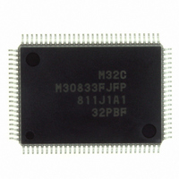
M30833FJFP#U3 Renesas Electronics America, M30833FJFP#U3 Datasheet - Page 255

M30833FJFP#U3
Manufacturer Part Number
M30833FJFP#U3
Description
IC M32C/83 MCU FLASH 100QFP
Manufacturer
Renesas Electronics America
Series
M16C™ M32C/80r
Datasheets
1.M3087BFLGPU3.pdf
(364 pages)
2.M30833FJGPU3.pdf
(96 pages)
3.M30833FJGPU3.pdf
(529 pages)
Specifications of M30833FJFP#U3
Core Processor
M32C/80
Core Size
16/32-Bit
Speed
32MHz
Connectivity
CAN, I²C, IEBus, SIO, UART/USART
Peripherals
DMA, WDT
Number Of I /o
85
Program Memory Size
512KB (512K x 8)
Program Memory Type
FLASH
Ram Size
31K x 8
Voltage - Supply (vcc/vdd)
3 V ~ 5.5 V
Data Converters
A/D 26x10b; D/A 2x8b
Oscillator Type
Internal
Operating Temperature
-40°C ~ 85°C
Package / Case
100-QFP
For Use With
R0K330879S001BE - KIT DEV RSK M32C/87R0K330879S000BE - KIT DEV RSK M32C/87
Lead Free Status / RoHS Status
Lead free / RoHS Compliant
Eeprom Size
-
Available stocks
Company
Part Number
Manufacturer
Quantity
Price
- Current page: 255 of 529
- Download datasheet (5Mb)
R
R
M
e
E
. v
3
J
Figure 17.4 AD0CON2 Register, AD00 to AD07 Registers
0
2
1
9
C
3 .
B
8 /
0
1
0
3
3
J
G
4
a
b15
A/D0 Register i (i =0 to 7)
0 -
n
o r
A/D0 Control Register 2
b7
3 .
1
NOTES:
u
, 1
3
p
1
b6
1. When the AD0CON2 register is rewritten during the A/D conversion, the conversion result is
2. Do not set the APS1 and APS0 bits to "1" while either A/D0 or A/D1 is operating.
3. The PST bit is enabled when the TRG bit in the AD0CON0 register is set to "0" (software trigger).
4. Set both A/D0 and A/D1 to the same setting.
5. If the ADS bit is set to "1", do not select single sweep mode or repeat sweep mode as the A/D
2
(
indeterminate.
Do not set the PST bit to "1" when the TRG bit is set to "1" (external trigger).
operation mode.
0
M
b5
0
3
6
b8
2
b4
C
b7
Page 230
8 /
b3
0 0 0
, 3
b2
M
b1
3
2
b0
C
b0
f o
8 /
8 low-order bits in an A/D conversion result
In 10-bit mode
In 8-bit mode
4
Nothing is assigned. When write, set to "0".
When read, its content is indeterminate.
(b3 - b1)
8
3
Symbol
TRG1
TRG0
Symbol
AD00 to AD02
AD03 to AD05
AD06 to AD07
8
) T
SMP
ADS
PST
Bit
Symbol
AD0CON2
(1)
A/D Conversion
Method Select Bit
Reserved Bit
A/D Channel Replace
Select Bit
External Trigger
Request Cause
Select Bit
Simultaneous
Start Bit
Address
0381
0387
038D
Bit Name
: 2 high-order bits in an A/D conversion result
: When read, its contents is indeterminate.
(2, 3, 4)
(2)
16
16
16
Address
0394
- 0380
- 0386
- 038C
16
16
16
16
, 0383
, 0389
, 038F
Function
0 : Without the sample and hold function
1 : With the sample and hold function
Set to "0"
0 : Disables channel replacement
1 : Enables channel replacement
b6 b5
When this bit is set to "1", A/D0 and
A/D1 start conversions simultaneously.
When read, its content is indeterminate.
0 0 : Selects AD
0 1 : Selects a timer B2 interrupt
1 0 : Selects the intelligent I/O group 2
1 1 : Do not set to this value
16
16
16
- 0382
- 0388
request of the three-phase motor
control timer functions (after
ICTB2 counter completes
counting)
channel 1 interrupt
- 038E
16
16
16
, 0385
, 038B
After Reset
X000 0000
TRG
Function
16
16
- 0384
- 038A
2
16
16
Indeterminate
Indeterminate
After Reset
Indeterminate
(5)
17. A/D Converter
RW
RO
RO
RW
RW
RW
RW
RW
RW
WO
Related parts for M30833FJFP#U3
Image
Part Number
Description
Manufacturer
Datasheet
Request
R

Part Number:
Description:
KIT STARTER FOR M16C/29
Manufacturer:
Renesas Electronics America
Datasheet:

Part Number:
Description:
KIT STARTER FOR R8C/2D
Manufacturer:
Renesas Electronics America
Datasheet:

Part Number:
Description:
R0K33062P STARTER KIT
Manufacturer:
Renesas Electronics America
Datasheet:

Part Number:
Description:
KIT STARTER FOR R8C/23 E8A
Manufacturer:
Renesas Electronics America
Datasheet:

Part Number:
Description:
KIT STARTER FOR R8C/25
Manufacturer:
Renesas Electronics America
Datasheet:

Part Number:
Description:
KIT STARTER H8S2456 SHARPE DSPLY
Manufacturer:
Renesas Electronics America
Datasheet:

Part Number:
Description:
KIT STARTER FOR R8C38C
Manufacturer:
Renesas Electronics America
Datasheet:

Part Number:
Description:
KIT STARTER FOR R8C35C
Manufacturer:
Renesas Electronics America
Datasheet:

Part Number:
Description:
KIT STARTER FOR R8CL3AC+LCD APPS
Manufacturer:
Renesas Electronics America
Datasheet:

Part Number:
Description:
KIT STARTER FOR RX610
Manufacturer:
Renesas Electronics America
Datasheet:

Part Number:
Description:
KIT STARTER FOR R32C/118
Manufacturer:
Renesas Electronics America
Datasheet:

Part Number:
Description:
KIT DEV RSK-R8C/26-29
Manufacturer:
Renesas Electronics America
Datasheet:

Part Number:
Description:
KIT STARTER FOR SH7124
Manufacturer:
Renesas Electronics America
Datasheet:

Part Number:
Description:
KIT STARTER FOR H8SX/1622
Manufacturer:
Renesas Electronics America
Datasheet:

Part Number:
Description:
KIT DEV FOR SH7203
Manufacturer:
Renesas Electronics America
Datasheet:


