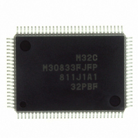
M30833FJFP#U3 Renesas Electronics America, M30833FJFP#U3 Datasheet - Page 261

M30833FJFP#U3
Manufacturer Part Number
M30833FJFP#U3
Description
IC M32C/83 MCU FLASH 100QFP
Manufacturer
Renesas Electronics America
Series
M16C™ M32C/80r
Datasheets
1.M3087BFLGPU3.pdf
(364 pages)
2.M30833FJGPU3.pdf
(96 pages)
3.M30833FJGPU3.pdf
(529 pages)
Specifications of M30833FJFP#U3
Core Processor
M32C/80
Core Size
16/32-Bit
Speed
32MHz
Connectivity
CAN, I²C, IEBus, SIO, UART/USART
Peripherals
DMA, WDT
Number Of I /o
85
Program Memory Size
512KB (512K x 8)
Program Memory Type
FLASH
Ram Size
31K x 8
Voltage - Supply (vcc/vdd)
3 V ~ 5.5 V
Data Converters
A/D 26x10b; D/A 2x8b
Oscillator Type
Internal
Operating Temperature
-40°C ~ 85°C
Package / Case
100-QFP
For Use With
R0K330879S001BE - KIT DEV RSK M32C/87R0K330879S000BE - KIT DEV RSK M32C/87
Lead Free Status / RoHS Status
Lead free / RoHS Compliant
Eeprom Size
-
Available stocks
Company
Part Number
Manufacturer
Quantity
Price
- Current page: 261 of 529
- Download datasheet (5Mb)
R
R
M
17.2 Function
e
E
. v
3
J
Table 17.8 Repeat Sweep Mode 1 Specifications
0
Function
Start Condition
Stop Condition
Interrupt Request Generation Timing Not generated
Analog Voltage Input Pins
Prioritized Pins
Reading of A/D Conversion Result The ADik register (k=0 to 7) corresponding to selected pins
2
17.1.5 Repeat Sweep Mode 1
17.2.1 Resolution Select Function
17.2.2 Sample and Hold
17.2.3 Trigger Select Function
1
9
C
3 .
B
In repeat sweep mode 1, analog voltage selectively applied to eight pins is repeatedly converted to a
digital code. Table 17.8 lists specifications of repeat sweep mode 1.
The BITS bit in the ADiCON1 (i=0, 1) register determines the resolution. When the BITS bit is set to "1"
(10-bit precision), the A/D conversion result is stored into bits 0 to 9 in the ADij register (j = 0 to 7). When
the BITS bit is set to "0" (8-bit precision), the A/D conversion result is stored into bits 0 to 7 in the ADij
register.
When the SMP bit in the ADiCON2 register is set to "1" (with the sample and hold function), A/D conver-
sion rate per pin increases to 28 Ø
The sample and hold function is available in all operating modes. Start the A/D conversion after selecting
whether the sample and hold function is to be used or not.
The TRG bit in the ADiCON0 register and the TRG1 to TRG0 bits in the ADiCON2 register determine the
trigger to start the A/D conversion. Table 17.9 lists settings of the trigger select function.
8 /
0
1
0
3
3
J
G
4
a
0 -
n
o r
3 .
1
u
, 1
3
Item
p
1
2
(
0
M
0
3
6
2
C
Page 236
8 /
, 3
M
3
2
C
f o
8 /
Select from AN
Analog voltage selectively applied to 8 pins selected by the SCAN1 to SCAN0 bits
in the ADiCON1 register (i=0,1) is repeatedly converted to a digital code.
Same as one-shot mode
program
ANj
pins)
Select from ANj
ANj
The ADST bit in the ADiCON1 register is set to "0" (A/D conversion stopped) by
4
e.g., When ANj
8
3
8
) T
0
0
ANj
to ANj
to ANj
digital code in the following order:
AD
0
cycles for 8-bit resolution and 33 Ø
7
3
ANj
(8 pins)
(4 pins)
0
1
0
(1 pin), AN
0
(j=0, 2, 15) (1 pin), ANj
is selected (j =none, 0, 2, 15), analog voltage is converted to a
ANj
0
0
ANij
to AN
2
Specification
1
(2 pins), AN
ANj
0
0
to ANj
ANj
3
0
AD
....... etc.
to AN
1
(2 pins), AN
cycles for 10-bit resolution.
2
(3 pins), or AN
0
17. A/D Converter
to AN
0
2
to AN
(3 pins),
3
(4
Related parts for M30833FJFP#U3
Image
Part Number
Description
Manufacturer
Datasheet
Request
R

Part Number:
Description:
KIT STARTER FOR M16C/29
Manufacturer:
Renesas Electronics America
Datasheet:

Part Number:
Description:
KIT STARTER FOR R8C/2D
Manufacturer:
Renesas Electronics America
Datasheet:

Part Number:
Description:
R0K33062P STARTER KIT
Manufacturer:
Renesas Electronics America
Datasheet:

Part Number:
Description:
KIT STARTER FOR R8C/23 E8A
Manufacturer:
Renesas Electronics America
Datasheet:

Part Number:
Description:
KIT STARTER FOR R8C/25
Manufacturer:
Renesas Electronics America
Datasheet:

Part Number:
Description:
KIT STARTER H8S2456 SHARPE DSPLY
Manufacturer:
Renesas Electronics America
Datasheet:

Part Number:
Description:
KIT STARTER FOR R8C38C
Manufacturer:
Renesas Electronics America
Datasheet:

Part Number:
Description:
KIT STARTER FOR R8C35C
Manufacturer:
Renesas Electronics America
Datasheet:

Part Number:
Description:
KIT STARTER FOR R8CL3AC+LCD APPS
Manufacturer:
Renesas Electronics America
Datasheet:

Part Number:
Description:
KIT STARTER FOR RX610
Manufacturer:
Renesas Electronics America
Datasheet:

Part Number:
Description:
KIT STARTER FOR R32C/118
Manufacturer:
Renesas Electronics America
Datasheet:

Part Number:
Description:
KIT DEV RSK-R8C/26-29
Manufacturer:
Renesas Electronics America
Datasheet:

Part Number:
Description:
KIT STARTER FOR SH7124
Manufacturer:
Renesas Electronics America
Datasheet:

Part Number:
Description:
KIT STARTER FOR H8SX/1622
Manufacturer:
Renesas Electronics America
Datasheet:

Part Number:
Description:
KIT DEV FOR SH7203
Manufacturer:
Renesas Electronics America
Datasheet:


