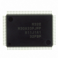
M30833FJFP#U3 Renesas Electronics America, M30833FJFP#U3 Datasheet - Page 308

M30833FJFP#U3
Manufacturer Part Number
M30833FJFP#U3
Description
IC M32C/83 MCU FLASH 100QFP
Manufacturer
Renesas Electronics America
Series
M16C™ M32C/80r
Datasheets
1.M3087BFLGPU3.pdf
(364 pages)
2.M30833FJGPU3.pdf
(96 pages)
3.M30833FJGPU3.pdf
(529 pages)
Specifications of M30833FJFP#U3
Core Processor
M32C/80
Core Size
16/32-Bit
Speed
32MHz
Connectivity
CAN, I²C, IEBus, SIO, UART/USART
Peripherals
DMA, WDT
Number Of I /o
85
Program Memory Size
512KB (512K x 8)
Program Memory Type
FLASH
Ram Size
31K x 8
Voltage - Supply (vcc/vdd)
3 V ~ 5.5 V
Data Converters
A/D 26x10b; D/A 2x8b
Oscillator Type
Internal
Operating Temperature
-40°C ~ 85°C
Package / Case
100-QFP
For Use With
R0K330879S001BE - KIT DEV RSK M32C/87R0K330879S000BE - KIT DEV RSK M32C/87
Lead Free Status / RoHS Status
Lead free / RoHS Compliant
Eeprom Size
-
Available stocks
Company
Part Number
Manufacturer
Quantity
Price
- Current page: 308 of 529
- Download datasheet (5Mb)
R
R
M
e
E
3
. v
J
2
0
Table 21.12 Bit Modulation PWM Output Mode Specifications
Output Waveform
Waveform Output Start Condition
Waveform Output Stop Condition
Interrupt Request
OUTCij Pin
Selectable Function
NOTES:
Table 21.13. Number of Modulated Spans and Minimum Resolution Bit Width Extended Span t
21.3.4 Bit Modulation PWM Output Mode (Group 2 and 3)
Number of Modulated Spans
00 0000 0000
00 0000 0001
00 0000 0010
00 0000 0100
00 0000 1000
10 0000 0000
1
C
9
3 .
B
In bit modulation PWM output mode, PWM output has a 16-bit resolution. Pulses are output in repetitive
cycles, each cycle consisting of span t repeated 1024 times. Span t, itself, has a cycle of
high-order bits in the GiPOj register (i=2 to 3; j=0 to 7) determine the "L" base width. The 10 low-order bits
determine the number of span t, within a cycle, in which "L" width is extended by the minimum resolution bit
width (1 clock cycle). If the INV bit is set to "1" (output is inversed), the level of the waveform being output
is inversed.
Table 21.12 lists specifications of bit modulation PWM output mode. Table 21.13 lists the number of
modulated span and minimum resolution bit width altered span t. Figure 21.27 shows an example of bit
modulation PWM mode operation.
1. Set the RST2 to RST0 bits in the GiBCR1 register to "000
2. When the INV bit in the GiPOCRj register is set to "1" (output inversed), the "L" width and "H" width are inversed.
8 /
0
1
3
0
3
J
G
4
a
0 -
n
o r
3 .
1
u
, 1
3
p
Item
1
2
2
2
2
2
2
2
(
M
0
0
(1,2)
3
6
2
C
Page 283
8 /
, 3
M
3
2
C
f o
8 /
4
n: Setting values (six high-order bits) of the GiPOj register (i=2 to 3; j=0 to 7)
m: Setting values (ten low-order bits) of the GiPOj register 00
3
Average "L" output width:
Cycle of span t:
"L" width: of m spans
8
PWM-repeated cycle T:
The IFEj bit in the GiFE register is set to "1" (channel j function enabled)
The IFEj bit is set to "0" (channel j function disabled)
The POijR bit in the interrupt request register is set to "1" when the value of the
six low-order bits of the base timer matches those set in the six high-order bits
of the GiPOj register (see Figure 10.14).
Pulse signal output pin
• Default value set function : Set starting waveform output level
• Inversed output function : Waveform output level is inversed and output from
) T
8
the OUTCij pin
00
Specification
16
to 3F
Minimum Resolution Bit Width Extended Span t
none
t512
t256, t768
t128, t384, t640, t896
t64, t192, t320, t448, t576, t704, t832, t960
t1, t3, t5, t7,
16
f
BTi
n
f
64
BTi
of (1024-m) spans
65536
2
" when using the bit modulation PWM mode.
21. Intelligent I/O (Waveform Generation Function)
f
BTi
f
t1019, t1021, t1023
n+1
f
1
BTi
BTi
X (n+
(=
f
64
BTi
1024
m
X1024)
)
16
to 3FF
f
64
BTi
16
. The six
Related parts for M30833FJFP#U3
Image
Part Number
Description
Manufacturer
Datasheet
Request
R

Part Number:
Description:
KIT STARTER FOR M16C/29
Manufacturer:
Renesas Electronics America
Datasheet:

Part Number:
Description:
KIT STARTER FOR R8C/2D
Manufacturer:
Renesas Electronics America
Datasheet:

Part Number:
Description:
R0K33062P STARTER KIT
Manufacturer:
Renesas Electronics America
Datasheet:

Part Number:
Description:
KIT STARTER FOR R8C/23 E8A
Manufacturer:
Renesas Electronics America
Datasheet:

Part Number:
Description:
KIT STARTER FOR R8C/25
Manufacturer:
Renesas Electronics America
Datasheet:

Part Number:
Description:
KIT STARTER H8S2456 SHARPE DSPLY
Manufacturer:
Renesas Electronics America
Datasheet:

Part Number:
Description:
KIT STARTER FOR R8C38C
Manufacturer:
Renesas Electronics America
Datasheet:

Part Number:
Description:
KIT STARTER FOR R8C35C
Manufacturer:
Renesas Electronics America
Datasheet:

Part Number:
Description:
KIT STARTER FOR R8CL3AC+LCD APPS
Manufacturer:
Renesas Electronics America
Datasheet:

Part Number:
Description:
KIT STARTER FOR RX610
Manufacturer:
Renesas Electronics America
Datasheet:

Part Number:
Description:
KIT STARTER FOR R32C/118
Manufacturer:
Renesas Electronics America
Datasheet:

Part Number:
Description:
KIT DEV RSK-R8C/26-29
Manufacturer:
Renesas Electronics America
Datasheet:

Part Number:
Description:
KIT STARTER FOR SH7124
Manufacturer:
Renesas Electronics America
Datasheet:

Part Number:
Description:
KIT STARTER FOR H8SX/1622
Manufacturer:
Renesas Electronics America
Datasheet:

Part Number:
Description:
KIT DEV FOR SH7203
Manufacturer:
Renesas Electronics America
Datasheet:


