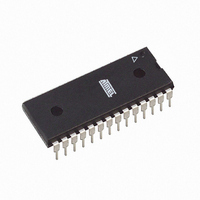
ATMEGA8L-8PU Atmel, ATMEGA8L-8PU Datasheet - Page 57

ATMEGA8L-8PU
Manufacturer Part Number
ATMEGA8L-8PU
Description
IC AVR MCU 8K 8MHZ 3V 28DIP
Manufacturer
Atmel
Series
AVR® ATmegar
Datasheets
1.ATMEGA8L-8MU.pdf
(25 pages)
2.ATMEGA8L-8MU.pdf
(302 pages)
3.ATMEGA8-16PU.pdf
(305 pages)
Specifications of ATMEGA8L-8PU
Core Processor
AVR
Core Size
8-Bit
Speed
8MHz
Connectivity
I²C, SPI, UART/USART
Peripherals
Brown-out Detect/Reset, POR, PWM, WDT
Number Of I /o
23
Program Memory Size
8KB (4K x 16)
Program Memory Type
FLASH
Eeprom Size
512 x 8
Ram Size
1K x 8
Voltage - Supply (vcc/vdd)
2.7 V ~ 5.5 V
Data Converters
A/D 6x10b
Oscillator Type
Internal
Operating Temperature
-40°C ~ 85°C
Package / Case
28-DIP (0.300", 7.62mm)
Cpu Family
ATmega
Device Core
AVR
Device Core Size
8b
Frequency (max)
8MHz
Interface Type
SPI/TWI/USART
Total Internal Ram Size
1KB
# I/os (max)
23
Number Of Timers - General Purpose
3
Operating Supply Voltage (typ)
3.3/5V
Operating Supply Voltage (max)
5.5V
Operating Supply Voltage (min)
2.7V
On-chip Adc
6-chx10-bit
Instruction Set Architecture
RISC
Operating Temp Range
-40C to 85C
Operating Temperature Classification
Industrial
Mounting
Through Hole
Pin Count
28
Package Type
PDIP
Processor Series
ATMEGA8x
Core
AVR8
Data Bus Width
8 bit
Data Ram Size
1 KB
Maximum Clock Frequency
8 MHz
Number Of Programmable I/os
23
Number Of Timers
3
Operating Supply Voltage
2.7 V to 5.5 V
Maximum Operating Temperature
+ 85 C
Mounting Style
Through Hole
3rd Party Development Tools
EWAVR, EWAVR-BL
Minimum Operating Temperature
- 40 C
Controller Family/series
AVR MEGA
No. Of I/o's
23
Eeprom Memory Size
512Byte
Ram Memory Size
1KB
Cpu Speed
8MHz
Rohs Compliant
Yes
For Use With
ATSTK600-TQFP32 - STK600 SOCKET/ADAPTER 32-TQFPATSTK600-DIP40 - STK600 SOCKET/ADAPTER 40-PDIP770-1007 - ISP 4PORT ATMEL AVR MCU SPI/JTAGATAVRISP2 - PROGRAMMER AVR IN SYSTEMATSTK500 - PROGRAMMER AVR STARTER KIT
Lead Free Status / RoHS Status
Lead free / RoHS Compliant
Available stocks
Company
Part Number
Manufacturer
Quantity
Price
Company:
Part Number:
ATMEGA8L-8PU
Manufacturer:
BROADCOM
Quantity:
101
Company:
Part Number:
ATMEGA8L-8PU
Manufacturer:
ATMEL
Quantity:
33 600
Part Number:
ATMEGA8L-8PU
Manufacturer:
ATMEL/爱特梅尔
Quantity:
20 000
Company:
Part Number:
ATMEGA8L-8PU-QS096
Manufacturer:
ATMEL
Quantity:
56
ATmega8(L)
inverting Oscillator amplifier. In this mode, a crystal Oscillator is connected to this pin,
and the pin can not be used as an I/O pin.
If PB6 is used as a clock pin, DDB6, PORTB6 and PINB6 will all read 0.
• SCK – Port B, Bit 5
SCK: Master Clock output, Slave Clock input pin for SPI channel. When the SPI is
enabled as a Slave, this pin is configured as an input regardless of the setting of DDB5.
When the SPI is enabled as a Master, the data direction of this pin is controlled by
DDB5. When the pin is forced by the SPI to be an input, the pull-up can still be con-
trolled by the PORTB5 bit.
• MISO – Port B, Bit 4
MISO: Master Data input, Slave Data output pin for SPI channel. When the SPI is
enabled as a Master, this pin is configured as an input regardless of the setting of
DDB4. When the SPI is enabled as a Slave, the data direction of this pin is controlled by
DDB4. When the pin is forced by the SPI to be an input, the pull-up can still be con-
trolled by the PORTB4 bit.
• MOSI/OC2 – Port B, Bit 3
MOSI: SPI Master Data output, Slave Data input for SPI channel. When the SPI is
enabled as a Slave, this pin is configured as an input regardless of the setting of DDB3.
When the SPI is enabled as a Master, the data direction of this pin is controlled by
DDB3. When the pin is forced by the SPI to be an input, the pull-up can still be con-
trolled by the PORTB3 bit.
OC2, Output Compare Match Output: The PB3 pin can serve as an external output for
the Timer/Counter2 Compare Match. The PB3 pin has to be configured as an output
(DDB3 set (one)) to serve this function. The OC2 pin is also the output pin for the PWM
mode timer function.
• SS/OC1B – Port B, Bit 2
SS: Slave Select input. When the SPI is enabled as a Slave, this pin is configured as an
input regardless of the setting of DDB2. As a Slave, the SPI is activated when this pin is
driven low. When the SPI is enabled as a Master, the data direction of this pin is con-
trolled by DDB2. When the pin is forced by the SPI to be an input, the pull-up can still be
controlled by the PORTB2 bit.
OC1B, Output Compare Match output: The PB2 pin can serve as an external output for
the Timer/Counter1 Compare Match B. The PB2 pin has to be configured as an output
(DDB2 set (one)) to serve this function. The OC1B pin is also the output pin for the PWM
mode timer function.
• OC1A – Port B, Bit 1
OC1A, Output Compare Match output: The PB1 pin can serve as an external output for
the Timer/Counter1 Compare Match A. The PB1 pin has to be configured as an output
(DDB1 set (one)) to serve this function. The OC1A pin is also the output pin for the PWM
mode timer function.
• ICP1 – Port B, Bit 0
ICP1 – Input Capture Pin: The PB0 pin can act as an Input Capture Pin for
Timer/Counter1.
Table 23 and Table 24 relate the alternate functions of Port B to the overriding signals
shown in Figure 25 on page 54. SPI MSTR INPUT and SPI SLAVE OUTPUT constitute
the MISO signal, while MOSI is divided into SPI MSTR OUTPUT and SPI SLAVE
INPUT.
57
2486O–AVR–10/04


