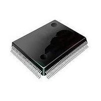
MC9S08DZ128MLL Freescale Semiconductor, MC9S08DZ128MLL Datasheet - Page 101

MC9S08DZ128MLL
Manufacturer Part Number
MC9S08DZ128MLL
Description
MCU 8BIT 128K FLASH 100-LQFP
Manufacturer
Freescale Semiconductor
Series
HCS08r
Datasheets
1.MC9S08DV96CLF.pdf
(458 pages)
2.MC9S08DV96CLF.pdf
(4 pages)
3.MC9S08DZ128CLF.pdf
(4 pages)
Specifications of MC9S08DZ128MLL
Core Processor
HCS08
Core Size
8-Bit
Speed
40MHz
Connectivity
CAN, I²C, LIN, SCI, SPI
Peripherals
LVD, POR, PWM, WDT
Number Of I /o
87
Program Memory Size
128KB (128K x 8)
Program Memory Type
FLASH
Eeprom Size
2K x 8
Ram Size
8K x 8
Voltage - Supply (vcc/vdd)
2.7 V ~ 5.5 V
Data Converters
A/D 24x12b
Oscillator Type
External
Operating Temperature
-40°C ~ 125°C
Package / Case
100-LQFP
Processor Series
S08DZ
Core
HCS08
Data Bus Width
8 bit
Data Ram Size
8 KB
Interface Type
CAN, I2C, SCI, SPI
Maximum Clock Frequency
40 MHz
Number Of Programmable I/os
88
Number Of Timers
3
Operating Supply Voltage
5.5 V
Maximum Operating Temperature
+ 125 C
Mounting Style
SMD/SMT
3rd Party Development Tools
EWS08
Development Tools By Supplier
DEMO9S08DZ60
Minimum Operating Temperature
- 40 C
On-chip Adc
12 bit, 24 Channel
Controller Family/series
HCS08
No. Of I/o's
87
Eeprom Memory Size
2KB
Ram Memory Size
8KB
Cpu Speed
40MHz
No. Of Timers
3
Digital Ic Case Style
LQFP
Rohs Compliant
Yes
Lead Free Status / RoHS Status
Lead free / RoHS Compliant
Available stocks
Company
Part Number
Manufacturer
Quantity
Price
Company:
Part Number:
MC9S08DZ128MLL
Manufacturer:
FREESCAL
Quantity:
300
Company:
Part Number:
MC9S08DZ128MLL
Manufacturer:
Freescale Semiconductor
Quantity:
10 000
- Current page: 101 of 458
- Download datasheet (5Mb)
Chapter 6
Parallel Input/Output Control
This section explains software controls related to parallel input/output (I/O) and pin control. The
MC9S08DZ128 Series has up to 11 parallel I/O ports which include a total of up to 87 I/O pins and one
input-only pin. See
external hardware considerations of these pins.
Many of these pins are shared with on-chip peripherals such as timer systems, communication systems, or
pin interrupts as shown in
functions so that when a peripheral is enabled, the I/O functions associated with the shared pins are
disabled.
After reset, the shared peripheral functions are disabled and the pins are configured as inputs
(PTxDDn = 0). The pin control functions for each pin are configured as follows: slew rate control enabled
(PTxSEn = 1), low drive strength selected (PTxDSn = 0), and internal pull-ups disabled (PTxPEn = 0).
6.1
Reading and writing of parallel I/Os are performed through the port data registers. The direction, either
input or output, is controlled through the port data direction registers. The parallel I/O port function for an
individual pin is illustrated in the block diagram shown in
The data direction control bit (PTxDDn) determines whether the output buffer for the associated pin is
enabled, and also controls the source for port data register reads. The input buffer for the associated pin is
always enabled unless the pin is enabled as an analog function or is an output-only pin.
When a shared digital function is enabled for a pin, the output buffer is controlled by the shared function.
However, the data direction register bit will continue to control the source for reads of the port data register.
When a shared analog function is enabled for a pin, both the input and output buffers are disabled. A value
of 0 is read for any port data bit where the bit is an input (PTxDDn = 0) and the input buffer is disabled.
In general, whenever a pin is shared with both an alternate digital function and an analog function, the
analog function has priority such that if both the digital and analog functions are enabled, the analog
function controls the pin.
Freescale Semiconductor
Port Data and Data Direction
Not all general-purpose I/O pins are available on all packages. To avoid
extra current drain from floating input pins, the user’s reset initialization
routine in the application program must either enable on-chip pull-up
devices or change the direction of unconnected pins to outputs so the pins
do not float.
Chapter 2, “Pins and
Table
2-1. The peripheral modules have priority over the general-purpose I/O
MC9S08DZ128 Series Data Sheet, Rev. 1
Connections,” for more information about pin assignments and
NOTE
Figure
6-1.
101
Related parts for MC9S08DZ128MLL
Image
Part Number
Description
Manufacturer
Datasheet
Request
R
Part Number:
Description:
Manufacturer:
Freescale Semiconductor, Inc
Datasheet:
Part Number:
Description:
Manufacturer:
Freescale Semiconductor, Inc
Datasheet:
Part Number:
Description:
Manufacturer:
Freescale Semiconductor, Inc
Datasheet:
Part Number:
Description:
Manufacturer:
Freescale Semiconductor, Inc
Datasheet:
Part Number:
Description:
Manufacturer:
Freescale Semiconductor, Inc
Datasheet:
Part Number:
Description:
Manufacturer:
Freescale Semiconductor, Inc
Datasheet:
Part Number:
Description:
Manufacturer:
Freescale Semiconductor, Inc
Datasheet:
Part Number:
Description:
Manufacturer:
Freescale Semiconductor, Inc
Datasheet:
Part Number:
Description:
Manufacturer:
Freescale Semiconductor, Inc
Datasheet:
Part Number:
Description:
Manufacturer:
Freescale Semiconductor, Inc
Datasheet:
Part Number:
Description:
Manufacturer:
Freescale Semiconductor, Inc
Datasheet:
Part Number:
Description:
Manufacturer:
Freescale Semiconductor, Inc
Datasheet:
Part Number:
Description:
Manufacturer:
Freescale Semiconductor, Inc
Datasheet:
Part Number:
Description:
Manufacturer:
Freescale Semiconductor, Inc
Datasheet:
Part Number:
Description:
Manufacturer:
Freescale Semiconductor, Inc
Datasheet:


