MC9S08DZ128MLL Freescale Semiconductor, MC9S08DZ128MLL Datasheet - Page 227
MC9S08DZ128MLL
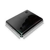
Manufacturer Part Number
MC9S08DZ128MLL
Description
MCU 8BIT 128K FLASH 100-LQFP
Manufacturer
Freescale Semiconductor
Series
HCS08r
Datasheets
1.MC9S08DV96CLF.pdf
(458 pages)
2.MC9S08DV96CLF.pdf
(4 pages)
3.MC9S08DZ128CLF.pdf
(4 pages)
Specifications of MC9S08DZ128MLL
Core Processor
HCS08
Core Size
8-Bit
Speed
40MHz
Connectivity
CAN, I²C, LIN, SCI, SPI
Peripherals
LVD, POR, PWM, WDT
Number Of I /o
87
Program Memory Size
128KB (128K x 8)
Program Memory Type
FLASH
Eeprom Size
2K x 8
Ram Size
8K x 8
Voltage - Supply (vcc/vdd)
2.7 V ~ 5.5 V
Data Converters
A/D 24x12b
Oscillator Type
External
Operating Temperature
-40°C ~ 125°C
Package / Case
100-LQFP
Processor Series
S08DZ
Core
HCS08
Data Bus Width
8 bit
Data Ram Size
8 KB
Interface Type
CAN, I2C, SCI, SPI
Maximum Clock Frequency
40 MHz
Number Of Programmable I/os
88
Number Of Timers
3
Operating Supply Voltage
5.5 V
Maximum Operating Temperature
+ 125 C
Mounting Style
SMD/SMT
3rd Party Development Tools
EWS08
Development Tools By Supplier
DEMO9S08DZ60
Minimum Operating Temperature
- 40 C
On-chip Adc
12 bit, 24 Channel
Controller Family/series
HCS08
No. Of I/o's
87
Eeprom Memory Size
2KB
Ram Memory Size
8KB
Cpu Speed
40MHz
No. Of Timers
3
Digital Ic Case Style
LQFP
Rohs Compliant
Yes
Lead Free Status / RoHS Status
Lead free / RoHS Compliant
Available stocks
Company
Part Number
Manufacturer
Quantity
Price
Company:

Part Number:
MC9S08DZ128MLL
Manufacturer:
FREESCAL
Quantity:
300
Company:
Part Number:
MC9S08DZ128MLL
Manufacturer:
Freescale Semiconductor
Quantity:
10 000


10.5
This section gives an example that provides some basic direction on how to initialize and configure the
ADC module. You can configure the module for 8-, 10-, or 12-bit resolution, single or continuous
conversion, and a polled or interrupt approach, among many other options. Refer to
Table
10.5.1
10.5.1.1
Before the ADC module can be used to complete conversions, an initialization procedure must be
performed. A typical sequence is as follows:
10.5.1.2
In this example, the ADC module is set up with interrupts enabled to perform a single 10-bit conversion
at low power with a long sample time on input channel 1, where the internal ADCK clock is derived from
the bus clock divided by 1.
ADCCFG = 0x98 (%10011000)
ADCSC2 = 0x00 (%00000000)
Freescale Semiconductor
1. Update the configuration register (ADCCFG) to select the input clock source and the divide ratio
2. Update status and control register 2 (ADCSC2) to select the conversion trigger (hardware or
3. Update status and control register 1 (ADCSC1) to select whether conversions will be continuous
10-8, and
used to generate the internal clock, ADCK. This register is also used for selecting sample time and
low-power configuration.
software) and compare function options, if enabled.
or completed only once, and to enable or disable conversion complete interrupts. The input channel
on which conversions will be performed is also selected here.
Initialization Information
Bit 7
Bit 6:5 ADIV
Bit 4
Bit 3:2 MODE
Bit 1:0 ADICLK
Bit 7
Bit 6
Bit 5
Bit 4
Bit 3:2
Bit 1:0
ADC Module Initialization Example
Initialization Sequence
Pseudo-Code Example
Hexadecimal values designated by a preceding 0x, binary values designated
by a preceding %, and decimal values have no preceding character.
Table 10-9
ADLPC
ADLSMP
ADACT
ADTRG
ACFE
ACFGT
for information used in this example.
1
00
1
10
00
0
0
0
0
00
00
MC9S08DZ128 Series Data Sheet, Rev. 1
Configures for low power (lowers maximum clock speed)
Sets the ADCK to the input clock ÷ 1
Configures for long sample time
Sets mode at 10-bit conversions
Selects bus clock as input clock source
Flag indicates if a conversion is in progress
Software trigger selected
Compare function disabled
Not used in this example
Reserved, always reads zero
Reserved for Freescale’s internal use; always write zero
NOTE
Chapter 10 Analog-to-Digital Converter (S08ADC12V1)
Table
10-7,
227
Related parts for MC9S08DZ128MLL
Image
Part Number
Description
Manufacturer
Datasheet
Request
R

Part Number:
Description:
Manufacturer:
Freescale Semiconductor, Inc
Datasheet:
Part Number:
Description:
Manufacturer:
Freescale Semiconductor, Inc
Datasheet:
Part Number:
Description:
Manufacturer:
Freescale Semiconductor, Inc
Datasheet:
Part Number:
Description:
Manufacturer:
Freescale Semiconductor, Inc
Datasheet:
Part Number:
Description:
Manufacturer:
Freescale Semiconductor, Inc
Datasheet:
Part Number:
Description:
Manufacturer:
Freescale Semiconductor, Inc
Datasheet:
Part Number:
Description:
Manufacturer:
Freescale Semiconductor, Inc
Datasheet:
Part Number:
Description:
Manufacturer:
Freescale Semiconductor, Inc
Datasheet:
Part Number:
Description:
Manufacturer:
Freescale Semiconductor, Inc
Datasheet:
Part Number:
Description:
Manufacturer:
Freescale Semiconductor, Inc
Datasheet:
Part Number:
Description:
Manufacturer:
Freescale Semiconductor, Inc
Datasheet:
Part Number:
Description:
Manufacturer:
Freescale Semiconductor, Inc
Datasheet:
Part Number:
Description:
Manufacturer:
Freescale Semiconductor, Inc
Datasheet:
Part Number:
Description:
Manufacturer:
Freescale Semiconductor, Inc
Datasheet:
Part Number:
Description:
Manufacturer:
Freescale Semiconductor, Inc
Datasheet: