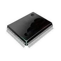
MC9S08DZ128MLL Freescale Semiconductor, MC9S08DZ128MLL Datasheet - Page 65

MC9S08DZ128MLL
Manufacturer Part Number
MC9S08DZ128MLL
Description
MCU 8BIT 128K FLASH 100-LQFP
Manufacturer
Freescale Semiconductor
Series
HCS08r
Datasheets
1.MC9S08DV96CLF.pdf
(458 pages)
2.MC9S08DV96CLF.pdf
(4 pages)
3.MC9S08DZ128CLF.pdf
(4 pages)
Specifications of MC9S08DZ128MLL
Core Processor
HCS08
Core Size
8-Bit
Speed
40MHz
Connectivity
CAN, I²C, LIN, SCI, SPI
Peripherals
LVD, POR, PWM, WDT
Number Of I /o
87
Program Memory Size
128KB (128K x 8)
Program Memory Type
FLASH
Eeprom Size
2K x 8
Ram Size
8K x 8
Voltage - Supply (vcc/vdd)
2.7 V ~ 5.5 V
Data Converters
A/D 24x12b
Oscillator Type
External
Operating Temperature
-40°C ~ 125°C
Package / Case
100-LQFP
Processor Series
S08DZ
Core
HCS08
Data Bus Width
8 bit
Data Ram Size
8 KB
Interface Type
CAN, I2C, SCI, SPI
Maximum Clock Frequency
40 MHz
Number Of Programmable I/os
88
Number Of Timers
3
Operating Supply Voltage
5.5 V
Maximum Operating Temperature
+ 125 C
Mounting Style
SMD/SMT
3rd Party Development Tools
EWS08
Development Tools By Supplier
DEMO9S08DZ60
Minimum Operating Temperature
- 40 C
On-chip Adc
12 bit, 24 Channel
Controller Family/series
HCS08
No. Of I/o's
87
Eeprom Memory Size
2KB
Ram Memory Size
8KB
Cpu Speed
40MHz
No. Of Timers
3
Digital Ic Case Style
LQFP
Rohs Compliant
Yes
Lead Free Status / RoHS Status
Lead free / RoHS Compliant
Available stocks
Company
Part Number
Manufacturer
Quantity
Price
Company:
Part Number:
MC9S08DZ128MLL
Manufacturer:
FREESCAL
Quantity:
300
Company:
Part Number:
MC9S08DZ128MLL
Manufacturer:
Freescale Semiconductor
Quantity:
10 000
- Current page: 65 of 458
- Download datasheet (5Mb)
address of the FLASH memory location to be addressed. When accessing data using LBP, the contents of
LAP2:LAP0 will increment after the read or write is complete.
Accessing LBP does the same thing as accessing LWP. The MMU register ordering of LWP followed by
LBP, allow the user to access data by words using the LDHX or STHX instructions with the address of the
LWP register.
4.4.3.5
This register is one of three data registers that the user can use to access any FLASH memory location in
the extended address map. When LB is accessed the contents of LAP2:LAP0 make up the extended
address of the FLASH memory location to be addressed.
4.4.3.6
The user can increase or decrease the contents of LAP2:LAP0 by writing a 2s complement value to
LAPAB. The value written will be added to the current contents of LAP2:LAP0.
Freescale Semiconductor
D7:D0
D7:D0
Field
Field
7:0
7:0
Reset:
Reset:
W
W
R
R
Reads of this register will first return the data value pointed to by the linear address pointer, LAP2:LAP0 and then
will increment LAP2:LAP0. Writes to this register will first write the data value to the memory location specified
by the linear address pointer and then will increment LAP2:LAP0. Writes to this register are most commonly used
when writing to the FLASH block(s) during programming.
Reads of this register returns the data value pointed to by the linear address pointer, LAP2:LAP0. Writes to this
register will write the data value to the memory location specified by the linear address pointer. Writes to this
register are most commonly used when writing to the FLASH block(s) during programming.
Linear Byte Register (LB)
Linear Address Pointer Add Byte Register (LAPAB)
D7
D7
0
0
7
7
Table 4-9. Linear Byte Post Increment Register Field Descriptions
Figure 4-8. Linear Byte Post Increment Register (LBP)
Table 4-10. Linear Data Register Field Descriptions
D6
D6
0
0
6
6
Figure 4-9. Linear Byte Register (LB)
MC9S08DZ128 Series Data Sheet, Rev. 1
D5
D5
5
0
5
0
D4
D4
0
0
4
4
Description
Description
D3
D3
0
0
3
3
D2
D2
0
0
2
2
D1
D1
0
0
1
1
Chapter 4 Memory
D0
D0
0
0
0
0
65
Related parts for MC9S08DZ128MLL
Image
Part Number
Description
Manufacturer
Datasheet
Request
R
Part Number:
Description:
Manufacturer:
Freescale Semiconductor, Inc
Datasheet:
Part Number:
Description:
Manufacturer:
Freescale Semiconductor, Inc
Datasheet:
Part Number:
Description:
Manufacturer:
Freescale Semiconductor, Inc
Datasheet:
Part Number:
Description:
Manufacturer:
Freescale Semiconductor, Inc
Datasheet:
Part Number:
Description:
Manufacturer:
Freescale Semiconductor, Inc
Datasheet:
Part Number:
Description:
Manufacturer:
Freescale Semiconductor, Inc
Datasheet:
Part Number:
Description:
Manufacturer:
Freescale Semiconductor, Inc
Datasheet:
Part Number:
Description:
Manufacturer:
Freescale Semiconductor, Inc
Datasheet:
Part Number:
Description:
Manufacturer:
Freescale Semiconductor, Inc
Datasheet:
Part Number:
Description:
Manufacturer:
Freescale Semiconductor, Inc
Datasheet:
Part Number:
Description:
Manufacturer:
Freescale Semiconductor, Inc
Datasheet:
Part Number:
Description:
Manufacturer:
Freescale Semiconductor, Inc
Datasheet:
Part Number:
Description:
Manufacturer:
Freescale Semiconductor, Inc
Datasheet:
Part Number:
Description:
Manufacturer:
Freescale Semiconductor, Inc
Datasheet:
Part Number:
Description:
Manufacturer:
Freescale Semiconductor, Inc
Datasheet:


