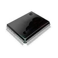
MC9S08DZ128MLL Freescale Semiconductor, MC9S08DZ128MLL Datasheet - Page 401

MC9S08DZ128MLL
Manufacturer Part Number
MC9S08DZ128MLL
Description
MCU 8BIT 128K FLASH 100-LQFP
Manufacturer
Freescale Semiconductor
Series
HCS08r
Datasheets
1.MC9S08DV96CLF.pdf
(458 pages)
2.MC9S08DV96CLF.pdf
(4 pages)
3.MC9S08DZ128CLF.pdf
(4 pages)
Specifications of MC9S08DZ128MLL
Core Processor
HCS08
Core Size
8-Bit
Speed
40MHz
Connectivity
CAN, I²C, LIN, SCI, SPI
Peripherals
LVD, POR, PWM, WDT
Number Of I /o
87
Program Memory Size
128KB (128K x 8)
Program Memory Type
FLASH
Eeprom Size
2K x 8
Ram Size
8K x 8
Voltage - Supply (vcc/vdd)
2.7 V ~ 5.5 V
Data Converters
A/D 24x12b
Oscillator Type
External
Operating Temperature
-40°C ~ 125°C
Package / Case
100-LQFP
Processor Series
S08DZ
Core
HCS08
Data Bus Width
8 bit
Data Ram Size
8 KB
Interface Type
CAN, I2C, SCI, SPI
Maximum Clock Frequency
40 MHz
Number Of Programmable I/os
88
Number Of Timers
3
Operating Supply Voltage
5.5 V
Maximum Operating Temperature
+ 125 C
Mounting Style
SMD/SMT
3rd Party Development Tools
EWS08
Development Tools By Supplier
DEMO9S08DZ60
Minimum Operating Temperature
- 40 C
On-chip Adc
12 bit, 24 Channel
Controller Family/series
HCS08
No. Of I/o's
87
Eeprom Memory Size
2KB
Ram Memory Size
8KB
Cpu Speed
40MHz
No. Of Timers
3
Digital Ic Case Style
LQFP
Rohs Compliant
Yes
Lead Free Status / RoHS Status
Lead free / RoHS Compliant
Available stocks
Company
Part Number
Manufacturer
Quantity
Price
Company:
Part Number:
MC9S08DZ128MLL
Manufacturer:
FREESCAL
Quantity:
300
Company:
Part Number:
MC9S08DZ128MLL
Manufacturer:
Freescale Semiconductor
Quantity:
10 000
- Current page: 401 of 458
- Download datasheet (5Mb)
18.3.3.8
1
Freescale Semiconductor
end-run
Module Base + 0x0007
end-run
Bits 15–8
or non-
In the case of an end-trace to reset where DBGEN=1 and BEGIN=0, the bits in this register do not change after reset.
Bits 7–0
Reset
Field
Field
POR
W
R
1
FIFO High Data Bits — The FIFO High data bits provide access to bits [15:8] of data in the FIFO. This register
is not used in event only modes and will read a $00 for valid FIFO words.
Bit 7
FIFO Low Data Bits — The FIFO Low data bits contain the least significant byte of data in the FIFO. When
reading FIFO words, read DBGFX and DBGFH before reading DBGFL because reading DBGFL causes the
FIFO pointers to advance to the next FIFO location. In event-only modes, there is no useful information in DBGFX
and DBGFH so it is not necessary to read them before reading DBGFL.
Debug FIFO Low Register (DBGFL)
U
0
7
= Unimplemented or Reserved
Bit 6
U
0
6
Figure 18-9. Debug FIFO Low Register (DBGFL)
Table 18-10. DBGFL Field Descriptions
Table 18-9. DBGFH Field Descriptions
MC9S08DZ128 Series Data Sheet, Rev. 1
Bit 5
U
0
5
Bit 4
U
0
4
Description
Description
Bit 3
U
0
3
Chapter 18 Debug Module (S08DBGV3) (128K)
Bit 2
U
0
2
Bit 1
U
0
1
Bit 0
U
0
0
401
Related parts for MC9S08DZ128MLL
Image
Part Number
Description
Manufacturer
Datasheet
Request
R
Part Number:
Description:
Manufacturer:
Freescale Semiconductor, Inc
Datasheet:
Part Number:
Description:
Manufacturer:
Freescale Semiconductor, Inc
Datasheet:
Part Number:
Description:
Manufacturer:
Freescale Semiconductor, Inc
Datasheet:
Part Number:
Description:
Manufacturer:
Freescale Semiconductor, Inc
Datasheet:
Part Number:
Description:
Manufacturer:
Freescale Semiconductor, Inc
Datasheet:
Part Number:
Description:
Manufacturer:
Freescale Semiconductor, Inc
Datasheet:
Part Number:
Description:
Manufacturer:
Freescale Semiconductor, Inc
Datasheet:
Part Number:
Description:
Manufacturer:
Freescale Semiconductor, Inc
Datasheet:
Part Number:
Description:
Manufacturer:
Freescale Semiconductor, Inc
Datasheet:
Part Number:
Description:
Manufacturer:
Freescale Semiconductor, Inc
Datasheet:
Part Number:
Description:
Manufacturer:
Freescale Semiconductor, Inc
Datasheet:
Part Number:
Description:
Manufacturer:
Freescale Semiconductor, Inc
Datasheet:
Part Number:
Description:
Manufacturer:
Freescale Semiconductor, Inc
Datasheet:
Part Number:
Description:
Manufacturer:
Freescale Semiconductor, Inc
Datasheet:
Part Number:
Description:
Manufacturer:
Freescale Semiconductor, Inc
Datasheet:


