MC9S12C32CFAE16 Freescale Semiconductor, MC9S12C32CFAE16 Datasheet - Page 108
MC9S12C32CFAE16
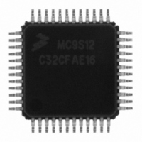
Manufacturer Part Number
MC9S12C32CFAE16
Description
IC MCU 32K FLASH 16MHZ 48-LQFP
Manufacturer
Freescale Semiconductor
Series
HCS12r
Datasheets
1.MC9S12GC16MFUE.pdf
(690 pages)
2.MC9S12C96CFUER.pdf
(26 pages)
3.MC9S12C32CFAE25.pdf
(2 pages)
Specifications of MC9S12C32CFAE16
Core Processor
HCS12
Core Size
16-Bit
Speed
16MHz
Connectivity
CAN, EBI/EMI, SCI, SPI
Peripherals
POR, PWM, WDT
Number Of I /o
31
Program Memory Size
32KB (32K x 8)
Program Memory Type
FLASH
Ram Size
2K x 8
Voltage - Supply (vcc/vdd)
2.35 V ~ 5.5 V
Data Converters
A/D 8x10b
Oscillator Type
Internal
Operating Temperature
-40°C ~ 85°C
Package / Case
48-LQFP
Cpu Family
HCS12
Device Core Size
16b
Frequency (max)
16MHz
Interface Type
CAN/SCI/SPI
Total Internal Ram Size
2KB
# I/os (max)
31
Number Of Timers - General Purpose
8
Operating Supply Voltage (typ)
2.5/5V
Operating Supply Voltage (max)
2.75/5.5V
Operating Supply Voltage (min)
2.35/2.97V
On-chip Adc
8-chx10-bit
Instruction Set Architecture
CISC
Operating Temp Range
-40C to 85C
Operating Temperature Classification
Industrial
Mounting
Surface Mount
Pin Count
48
Package Type
LQFP
Package
48LQFP
Family Name
HCS12
Maximum Speed
16 MHz
Operating Supply Voltage
2.5|5 V
Data Bus Width
16 Bit
Number Of Programmable I/os
31
Number Of Timers
8
For Use With
CML12C32SLK - KIT STUDENT LEARNING 16BIT HCS12
Lead Free Status / RoHS Status
Lead free / RoHS Compliant
Eeprom Size
-
Lead Free Status / Rohs Status
Compliant
Available stocks
Company
Part Number
Manufacturer
Quantity
Price

Company:
Part Number:
MC9S12C32CFAE16
Manufacturer:
Freescale Semiconductor
Quantity:
10 000


Chapter 2 Port Integration Module (PIM9C32) Block Description
2.6
Port P and J generate a separate edge sensitive interrupt if enabled.
2.6.1
2.6.2
The PIM can generate wake-up interrupts from STOP on port P and J. For other sources of external
interrupts please refer to the respective Block User Guide.
2.7
It is not recommended to write PORTx and DDRx in a word access. When changing the register pins from
inputs to outputs, the data may have extra transitions during the write access. Initialize the port data register
before enabling the outputs.
Power consumption will increase the more the voltages on general purpose input pins deviate from the
supply voltages towards mid-range because the digital input buffers operate in the linear region.
108
BKGD pin
Interrupts
Application Information
Port
Interrupt Sources
Interrupt Source
Recovery from STOP
M
T
S
P
A
B
E
J
Vector addresses and their relative interrupt priority are determined at the
MCU level.
Port P
Port J
Data Direction
Input
Input
Input
Input
Input
Table 2-40. Port Integration Module Interrupt Sources
Table 2-39. Port Reset State Summary
Interrupt Flag
MC9S12C-Family / MC9S12GC-Family
PIFP[7:0]
PIFJ[7:6]
Pull Mode
Pull up
Pull up
Hi-z
Hi-z
Hi-z
Refer to MEBI Block Guide for details.
Refer to BDM Block Guide for details.
Rev 01.24
NOTE
Reduced Drive
Reset States
Disabled
Disabled
Disabled
Disabled
Disabled
Local Enable
PIEP[7:0]
PIEJ[7:6]
Wired-OR Mode
Disabled
Disabled
n/a
n/a
n/a
Global (CCR) Mask
I Bit
I Bit
Freescale Semiconductor
Interrupt
Disabled
Disabled
n/a
n/a
n/a
Related parts for MC9S12C32CFAE16
Image
Part Number
Description
Manufacturer
Datasheet
Request
R

Part Number:
Description:
Manufacturer:
Freescale Semiconductor, Inc
Datasheet:
Part Number:
Description:
Manufacturer:
Freescale Semiconductor, Inc
Datasheet:
Part Number:
Description:
Manufacturer:
Freescale Semiconductor, Inc
Datasheet:
Part Number:
Description:
Manufacturer:
Freescale Semiconductor, Inc
Datasheet:
Part Number:
Description:
Manufacturer:
Freescale Semiconductor, Inc
Datasheet:
Part Number:
Description:
Manufacturer:
Freescale Semiconductor, Inc
Datasheet:
Part Number:
Description:
Manufacturer:
Freescale Semiconductor, Inc
Datasheet:
Part Number:
Description:
Manufacturer:
Freescale Semiconductor, Inc
Datasheet:
Part Number:
Description:
Manufacturer:
Freescale Semiconductor, Inc
Datasheet:
Part Number:
Description:
Manufacturer:
Freescale Semiconductor, Inc
Datasheet:
Part Number:
Description:
Manufacturer:
Freescale Semiconductor, Inc
Datasheet:
Part Number:
Description:
Manufacturer:
Freescale Semiconductor, Inc
Datasheet:
Part Number:
Description:
Manufacturer:
Freescale Semiconductor, Inc
Datasheet:
Part Number:
Description:
Manufacturer:
Freescale Semiconductor, Inc
Datasheet:
Part Number:
Description:
Manufacturer:
Freescale Semiconductor, Inc
Datasheet: