MC9S12C32CFAE16 Freescale Semiconductor, MC9S12C32CFAE16 Datasheet - Page 385
MC9S12C32CFAE16
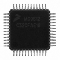
Manufacturer Part Number
MC9S12C32CFAE16
Description
IC MCU 32K FLASH 16MHZ 48-LQFP
Manufacturer
Freescale Semiconductor
Series
HCS12r
Datasheets
1.MC9S12GC16MFUE.pdf
(690 pages)
2.MC9S12C96CFUER.pdf
(26 pages)
3.MC9S12C32CFAE25.pdf
(2 pages)
Specifications of MC9S12C32CFAE16
Core Processor
HCS12
Core Size
16-Bit
Speed
16MHz
Connectivity
CAN, EBI/EMI, SCI, SPI
Peripherals
POR, PWM, WDT
Number Of I /o
31
Program Memory Size
32KB (32K x 8)
Program Memory Type
FLASH
Ram Size
2K x 8
Voltage - Supply (vcc/vdd)
2.35 V ~ 5.5 V
Data Converters
A/D 8x10b
Oscillator Type
Internal
Operating Temperature
-40°C ~ 85°C
Package / Case
48-LQFP
Cpu Family
HCS12
Device Core Size
16b
Frequency (max)
16MHz
Interface Type
CAN/SCI/SPI
Total Internal Ram Size
2KB
# I/os (max)
31
Number Of Timers - General Purpose
8
Operating Supply Voltage (typ)
2.5/5V
Operating Supply Voltage (max)
2.75/5.5V
Operating Supply Voltage (min)
2.35/2.97V
On-chip Adc
8-chx10-bit
Instruction Set Architecture
CISC
Operating Temp Range
-40C to 85C
Operating Temperature Classification
Industrial
Mounting
Surface Mount
Pin Count
48
Package Type
LQFP
Package
48LQFP
Family Name
HCS12
Maximum Speed
16 MHz
Operating Supply Voltage
2.5|5 V
Data Bus Width
16 Bit
Number Of Programmable I/os
31
Number Of Timers
8
For Use With
CML12C32SLK - KIT STUDENT LEARNING 16BIT HCS12
Lead Free Status / RoHS Status
Lead free / RoHS Compliant
Eeprom Size
-
Lead Free Status / Rohs Status
Compliant
Available stocks
Company
Part Number
Manufacturer
Quantity
Price

Company:
Part Number:
MC9S12C32CFAE16
Manufacturer:
Freescale Semiconductor
Quantity:
10 000


13.1.4
Figure 13-1
blocks.
13.2
The SCI module has a total of two external pins:
13.2.1
This pin serves as transmit data output of SCI.
13.2.2
This pin serves as receive data input of the SCI.
Freescale Semiconductor
RX DATA IN
BUS CLOCK
External Signal Description
Block Diagram
TXD-SCI Transmit Pin
RXD-SCI Receive Pin
is a high level block diagram of the SCI module, showing the interaction of various functional
GENERATOR
BAUD
MC9S12C-Family / MC9S12GC-Family
RECEIVE & WAKE UP CONTROL
Figure 13-1. SCI Block Diagram
RECEIVE SHIFT REGISTER
TRANSMIT SHIFT REGISTER
÷16
SCI DATA REGISTER
TRANSMIT CONTROL
SCI DATA REGISTER
Chapter 13 Serial Communications Interface (S12SCIV2) Block Description
Rev 01.24
DATA FORMAT CONTROL
TDRE IRQ
RDR/OR IRQ
TC IRQ
IDLE IRQ
TXDATA OUT
IRQ
TO CPU
385
Related parts for MC9S12C32CFAE16
Image
Part Number
Description
Manufacturer
Datasheet
Request
R

Part Number:
Description:
Manufacturer:
Freescale Semiconductor, Inc
Datasheet:
Part Number:
Description:
Manufacturer:
Freescale Semiconductor, Inc
Datasheet:
Part Number:
Description:
Manufacturer:
Freescale Semiconductor, Inc
Datasheet:
Part Number:
Description:
Manufacturer:
Freescale Semiconductor, Inc
Datasheet:
Part Number:
Description:
Manufacturer:
Freescale Semiconductor, Inc
Datasheet:
Part Number:
Description:
Manufacturer:
Freescale Semiconductor, Inc
Datasheet:
Part Number:
Description:
Manufacturer:
Freescale Semiconductor, Inc
Datasheet:
Part Number:
Description:
Manufacturer:
Freescale Semiconductor, Inc
Datasheet:
Part Number:
Description:
Manufacturer:
Freescale Semiconductor, Inc
Datasheet:
Part Number:
Description:
Manufacturer:
Freescale Semiconductor, Inc
Datasheet:
Part Number:
Description:
Manufacturer:
Freescale Semiconductor, Inc
Datasheet:
Part Number:
Description:
Manufacturer:
Freescale Semiconductor, Inc
Datasheet:
Part Number:
Description:
Manufacturer:
Freescale Semiconductor, Inc
Datasheet:
Part Number:
Description:
Manufacturer:
Freescale Semiconductor, Inc
Datasheet:
Part Number:
Description:
Manufacturer:
Freescale Semiconductor, Inc
Datasheet: