MC9S12C32CFAE16 Freescale Semiconductor, MC9S12C32CFAE16 Datasheet - Page 374
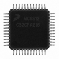
MC9S12C32CFAE16
Manufacturer Part Number
MC9S12C32CFAE16
Description
IC MCU 32K FLASH 16MHZ 48-LQFP
Manufacturer
Freescale Semiconductor
Series
HCS12r
Datasheets
1.MC9S12GC16MFUE.pdf
(690 pages)
2.MC9S12C96CFUER.pdf
(26 pages)
3.MC9S12C32CFAE25.pdf
(2 pages)
Specifications of MC9S12C32CFAE16
Core Processor
HCS12
Core Size
16-Bit
Speed
16MHz
Connectivity
CAN, EBI/EMI, SCI, SPI
Peripherals
POR, PWM, WDT
Number Of I /o
31
Program Memory Size
32KB (32K x 8)
Program Memory Type
FLASH
Ram Size
2K x 8
Voltage - Supply (vcc/vdd)
2.35 V ~ 5.5 V
Data Converters
A/D 8x10b
Oscillator Type
Internal
Operating Temperature
-40°C ~ 85°C
Package / Case
48-LQFP
Cpu Family
HCS12
Device Core Size
16b
Frequency (max)
16MHz
Interface Type
CAN/SCI/SPI
Total Internal Ram Size
2KB
# I/os (max)
31
Number Of Timers - General Purpose
8
Operating Supply Voltage (typ)
2.5/5V
Operating Supply Voltage (max)
2.75/5.5V
Operating Supply Voltage (min)
2.35/2.97V
On-chip Adc
8-chx10-bit
Instruction Set Architecture
CISC
Operating Temp Range
-40C to 85C
Operating Temperature Classification
Industrial
Mounting
Surface Mount
Pin Count
48
Package Type
LQFP
Package
48LQFP
Family Name
HCS12
Maximum Speed
16 MHz
Operating Supply Voltage
2.5|5 V
Data Bus Width
16 Bit
Number Of Programmable I/os
31
Number Of Timers
8
For Use With
CML12C32SLK - KIT STUDENT LEARNING 16BIT HCS12
Lead Free Status / RoHS Status
Lead free / RoHS Compliant
Eeprom Size
-
Lead Free Status / Rohs Status
Compliant
Available stocks
Company
Part Number
Manufacturer
Quantity
Price

Company:
Part Number:
MC9S12C32CFAE16
Manufacturer:
Freescale Semiconductor
Quantity:
10 000


Chapter 12 Pulse-Width Modulator (PWM8B6CV1) Block Description
12.4.1.3
Each PWM channel has the capability of selecting one of two clocks. For channels 0, 1, 4, and 5 the clock
choices are clock A or clock SA. For channels 2 and 3 the choices are clock B or clock SB. The clock
selection is done with the PCLKx control bits in the PWMCLK register.
12.4.2
The main part of the PWM module are the actual timers. Each of the timer channels has a counter, a period
register and a duty register (each are 8 bit). The waveform output period is controlled by a match between
the period register and the value in the counter. The duty is controlled by a match between the duty register
and the counter value and causes the state of the output to change during the period. The starting polarity
of the output is also selectable on a per channel basis.
374
Clock Source
PWMEx
(clock edge sync)
PWM Channel Timers
Clock Select
GATE
Changing clock control bits while channels are operating can cause
irregularities in the PWM outputs.
up/down
reset
Figure 12-35. PWM Timer Channel Block Diagram
8-Bit Counter
PWMCNTx
Q
Q
T
R
MC9S12C-Family / MC9S12GC-Family
Rev 01.24
NOTE
Figure 12-35
8-Bit Compare =
8-Bit Compare =
PWMDTYx
PWMPERx
CAEx
shows a block diagram for PWM timer.
T
R
Q
Q
PPOLx
M
U
X
From Port PWMP
Data Register
Freescale Semiconductor
M
U
X
To Pin
Driver
Related parts for MC9S12C32CFAE16
Image
Part Number
Description
Manufacturer
Datasheet
Request
R

Part Number:
Description:
Manufacturer:
Freescale Semiconductor, Inc
Datasheet:
Part Number:
Description:
Manufacturer:
Freescale Semiconductor, Inc
Datasheet:
Part Number:
Description:
Manufacturer:
Freescale Semiconductor, Inc
Datasheet:
Part Number:
Description:
Manufacturer:
Freescale Semiconductor, Inc
Datasheet:
Part Number:
Description:
Manufacturer:
Freescale Semiconductor, Inc
Datasheet:
Part Number:
Description:
Manufacturer:
Freescale Semiconductor, Inc
Datasheet:
Part Number:
Description:
Manufacturer:
Freescale Semiconductor, Inc
Datasheet:
Part Number:
Description:
Manufacturer:
Freescale Semiconductor, Inc
Datasheet:
Part Number:
Description:
Manufacturer:
Freescale Semiconductor, Inc
Datasheet:
Part Number:
Description:
Manufacturer:
Freescale Semiconductor, Inc
Datasheet:
Part Number:
Description:
Manufacturer:
Freescale Semiconductor, Inc
Datasheet:
Part Number:
Description:
Manufacturer:
Freescale Semiconductor, Inc
Datasheet:
Part Number:
Description:
Manufacturer:
Freescale Semiconductor, Inc
Datasheet:
Part Number:
Description:
Manufacturer:
Freescale Semiconductor, Inc
Datasheet:
Part Number:
Description:
Manufacturer:
Freescale Semiconductor, Inc
Datasheet: