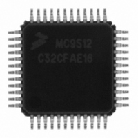
MC9S12C32CFAE16 Freescale Semiconductor, MC9S12C32CFAE16 Datasheet - Page 236

MC9S12C32CFAE16
Manufacturer Part Number
MC9S12C32CFAE16
Description
IC MCU 32K FLASH 16MHZ 48-LQFP
Manufacturer
Freescale Semiconductor
Series
HCS12r
Datasheets
1.MC9S12GC16MFUE.pdf
(690 pages)
2.MC9S12C96CFUER.pdf
(26 pages)
3.MC9S12C32CFAE25.pdf
(2 pages)
Specifications of MC9S12C32CFAE16
Core Processor
HCS12
Core Size
16-Bit
Speed
16MHz
Connectivity
CAN, EBI/EMI, SCI, SPI
Peripherals
POR, PWM, WDT
Number Of I /o
31
Program Memory Size
32KB (32K x 8)
Program Memory Type
FLASH
Ram Size
2K x 8
Voltage - Supply (vcc/vdd)
2.35 V ~ 5.5 V
Data Converters
A/D 8x10b
Oscillator Type
Internal
Operating Temperature
-40°C ~ 85°C
Package / Case
48-LQFP
Cpu Family
HCS12
Device Core Size
16b
Frequency (max)
16MHz
Interface Type
CAN/SCI/SPI
Total Internal Ram Size
2KB
# I/os (max)
31
Number Of Timers - General Purpose
8
Operating Supply Voltage (typ)
2.5/5V
Operating Supply Voltage (max)
2.75/5.5V
Operating Supply Voltage (min)
2.35/2.97V
On-chip Adc
8-chx10-bit
Instruction Set Architecture
CISC
Operating Temp Range
-40C to 85C
Operating Temperature Classification
Industrial
Mounting
Surface Mount
Pin Count
48
Package Type
LQFP
Package
48LQFP
Family Name
HCS12
Maximum Speed
16 MHz
Operating Supply Voltage
2.5|5 V
Data Bus Width
16 Bit
Number Of Programmable I/os
31
Number Of Timers
8
For Use With
CML12C32SLK - KIT STUDENT LEARNING 16BIT HCS12
Lead Free Status / RoHS Status
Lead free / RoHS Compliant
Eeprom Size
-
Lead Free Status / Rohs Status
Compliant
Available stocks
Company
Part Number
Manufacturer
Quantity
Price
Company:
Part Number:
MC9S12C32CFAE16
Manufacturer:
Freescale Semiconductor
Quantity:
10 000
- Current page: 236 of 690
- Download datasheet (4Mb)
Chapter 8 Analog-to-Digital Converter (ATD10B8C) Block Description
8.3.2.6
This register selects the type of conversion sequence and the analog input channels sampled. Writes to this
register will abort current conversion sequence and start a new conversion sequence.
Read: Anytime
Write: Anytime
236
Module Base + 0x0005
CC, CB, CA
Reset
DSGN
SCAN
MULT
Field
DJM
2–1
7
6
5
4
W
R
DJM
Result Register Data Justification — This bit controls justification of conversion data in the result registers.
See
0 Left justified data in the result registers
1 Right justified data in the result registers
Result Register Data Signed or Unsigned Representation — This bit selects between signed and unsigned
conversion data representation in the result registers. Signed data is represented as 2’s complement. Signed
data is not available in right justification. See
(ATDDRHx/ATDDRLx)”
0 Unsigned data representation in the result registers
1 Signed data representation in the result registers
Table 8-10
Table 8-11
signal range between 0 and 5.12 Volts.
Continuous Conversion Sequence Mode — This bit selects whether conversion sequences are performed
continuously or only once.
0 Single conversion sequence
1 Continuous conversion sequences (scan mode)
Multi-Channel Sample Mode — When MULT is 0, the ATD sequence controller samples only from the specified
analog input channel for an entire conversion sequence. The analog channel is selected by channel selection
code (control bits CC/CB/CA located in ATDCTL5). When MULT is 1, the ATD sequence controller samples
across channels. The number of channels sampled is determined by the sequence length value (S8C, S4C, S2C,
S1C). The first analog channel examined is determined by channel selection code (CC, CB, CA control bits);
subsequent channels sampled in the sequence are determined by incrementing the channel selection code.
0 Sample only one channel
1 Sample across several channels
Analog Input Channel Select Code — These bits select the analog input channel(s) whose signals are
sampled and converted to digital codes.
channels. In the case of single channel scans (MULT = 0), this selection code specified the channel examined.
In the case of multi-channel scans (MULT = 1), this selection code represents the first channel to be examined
in the conversion sequence. Subsequent channels are determined by incrementing channel selection code;
selection codes that reach the maximum value wrap around to the minimum value.
ATD Control Register 5 (ATDCTL5)
0
7
Section 8.3.2.13, “ATD Conversion Result Registers (ATDDRHx/ATDDRLx)”
= Unimplemented or Reserved
summarizes the result data formats available and how they are set up using the control bits.
illustrates the difference between the signed and unsigned, left justified output codes for an input
DSGN
0
6
Figure 8-8. ATD Control Register 5 (ATDCTL5)
for details.
Table 8-9. ATDCTL5 Field Descriptions
SCAN
MC9S12C-Family / MC9S12GC-Family
0
5
Table 8-12
MULT
Rev 01.24
Section 8.3.2.13, “ATD Conversion Result Registers
0
4
Description
lists the coding used to select the various analog input
0
0
3
CC
0
2
for details.
Freescale Semiconductor
CB
0
1
CA
0
0
Related parts for MC9S12C32CFAE16
Image
Part Number
Description
Manufacturer
Datasheet
Request
R
Part Number:
Description:
Manufacturer:
Freescale Semiconductor, Inc
Datasheet:
Part Number:
Description:
Manufacturer:
Freescale Semiconductor, Inc
Datasheet:
Part Number:
Description:
Manufacturer:
Freescale Semiconductor, Inc
Datasheet:
Part Number:
Description:
Manufacturer:
Freescale Semiconductor, Inc
Datasheet:
Part Number:
Description:
Manufacturer:
Freescale Semiconductor, Inc
Datasheet:
Part Number:
Description:
Manufacturer:
Freescale Semiconductor, Inc
Datasheet:
Part Number:
Description:
Manufacturer:
Freescale Semiconductor, Inc
Datasheet:
Part Number:
Description:
Manufacturer:
Freescale Semiconductor, Inc
Datasheet:
Part Number:
Description:
Manufacturer:
Freescale Semiconductor, Inc
Datasheet:
Part Number:
Description:
Manufacturer:
Freescale Semiconductor, Inc
Datasheet:
Part Number:
Description:
Manufacturer:
Freescale Semiconductor, Inc
Datasheet:
Part Number:
Description:
Manufacturer:
Freescale Semiconductor, Inc
Datasheet:
Part Number:
Description:
Manufacturer:
Freescale Semiconductor, Inc
Datasheet:
Part Number:
Description:
Manufacturer:
Freescale Semiconductor, Inc
Datasheet:
Part Number:
Description:
Manufacturer:
Freescale Semiconductor, Inc
Datasheet:


