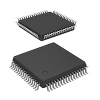
DF36054GFPJV Renesas Electronics America, DF36054GFPJV Datasheet - Page 386

DF36054GFPJV
Manufacturer Part Number
DF36054GFPJV
Description
MCU 3/5V 32K J-TEMP PB-FREE 64-L
Manufacturer
Renesas Electronics America
Series
H8® H8/300H Tinyr
Datasheet
1.DF36057GFZV.pdf
(594 pages)
Specifications of DF36054GFPJV
Core Processor
H8/300H
Core Size
16-Bit
Speed
20MHz
Connectivity
CAN, SCI, SSU
Peripherals
LVD, POR, PWM, WDT
Number Of I /o
45
Program Memory Size
32KB (32K x 8)
Program Memory Type
FLASH
Ram Size
2K x 8
Voltage - Supply (vcc/vdd)
3 V ~ 5.5 V
Data Converters
A/D 8x10b
Oscillator Type
Internal
Operating Temperature
-40°C ~ 85°C
Package / Case
64-LQFP
Lead Free Status / RoHS Status
Lead free / RoHS Compliant
Eeprom Size
-
- Current page: 386 of 594
- Download datasheet (4Mb)
Section 16 Synchronous Serial Communication Unit (SSU)
[Legend]
X: Don't care.
Rev. 4.00 Mar. 15, 2006 Page 352 of 556
REJ09B0026-0400
Bit
4
3
2
1
0
Bit Name
SOL
SOLP
SCKS
CSS1
CSS0
Initial
Value
0
1
0
0
0
R/W
R/W
R/W
R/W
R/W
R/W
Description
Serial Data Output Level Setting
Although the value in the last bit of transmit data is
retained in the serial data output after the end of
transmission, the output level of serial data can be
changed by manipulating this bit before or after
transmission. When the output level is changed, the
SOLP bit should be cleared to 0 and the MOV instruction
should be used. If this bit is written during data transfer,
erroneous operation may occur. Therefore this bit must
not be manipulated during transmission.
0: Shows serial data output level to low in reading.
1: Shows serial data output level to high in reading.
SOL Write Protect
When output level of serial data is changed, the MOV
instruction is used to set the SOL bit to 1 and clear this bit
to 0 or to clear the SOL bit and this bit to 0.
0: In writing, output level can be changed according to the
1: In reading, this bit is always read as 1. In writing, it
SSCK Pin Select
Selects whether the SSCK pin functions as a port or a
serial clock pin.
0: Functions as a port
1: Functions as a serial clock pin
SCS Pin Select
Selects whether the SCS pin functions as a port, an SCS
input, or SCS output. When the SSUMS bit in SSCRL is
0, the SCS pin functions as a port regardless of the
setting of this bit.
00: Functions as a port
01: Functions as an SCS input
1X: Functions as an SCS output (however, functions as
Changes serial data output level to low in writing
Changes serial data output level to high in writing
value of the SOL bit.
cannot be modified output level.
an SCS input before starting transfer)
Related parts for DF36054GFPJV
Image
Part Number
Description
Manufacturer
Datasheet
Request
R

Part Number:
Description:
KIT STARTER FOR M16C/29
Manufacturer:
Renesas Electronics America
Datasheet:

Part Number:
Description:
KIT STARTER FOR R8C/2D
Manufacturer:
Renesas Electronics America
Datasheet:

Part Number:
Description:
R0K33062P STARTER KIT
Manufacturer:
Renesas Electronics America
Datasheet:

Part Number:
Description:
KIT STARTER FOR R8C/23 E8A
Manufacturer:
Renesas Electronics America
Datasheet:

Part Number:
Description:
KIT STARTER FOR R8C/25
Manufacturer:
Renesas Electronics America
Datasheet:

Part Number:
Description:
KIT STARTER H8S2456 SHARPE DSPLY
Manufacturer:
Renesas Electronics America
Datasheet:

Part Number:
Description:
KIT STARTER FOR R8C38C
Manufacturer:
Renesas Electronics America
Datasheet:

Part Number:
Description:
KIT STARTER FOR R8C35C
Manufacturer:
Renesas Electronics America
Datasheet:

Part Number:
Description:
KIT STARTER FOR R8CL3AC+LCD APPS
Manufacturer:
Renesas Electronics America
Datasheet:

Part Number:
Description:
KIT STARTER FOR RX610
Manufacturer:
Renesas Electronics America
Datasheet:

Part Number:
Description:
KIT STARTER FOR R32C/118
Manufacturer:
Renesas Electronics America
Datasheet:

Part Number:
Description:
KIT DEV RSK-R8C/26-29
Manufacturer:
Renesas Electronics America
Datasheet:

Part Number:
Description:
KIT STARTER FOR SH7124
Manufacturer:
Renesas Electronics America
Datasheet:

Part Number:
Description:
KIT STARTER FOR H8SX/1622
Manufacturer:
Renesas Electronics America
Datasheet:

Part Number:
Description:
KIT DEV FOR SH7203
Manufacturer:
Renesas Electronics America
Datasheet:


