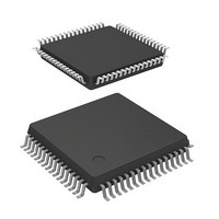
DF36054GFPJV Renesas Electronics America, DF36054GFPJV Datasheet - Page 398

DF36054GFPJV
Manufacturer Part Number
DF36054GFPJV
Description
MCU 3/5V 32K J-TEMP PB-FREE 64-L
Manufacturer
Renesas Electronics America
Series
H8® H8/300H Tinyr
Datasheet
1.DF36057GFZV.pdf
(594 pages)
Specifications of DF36054GFPJV
Core Processor
H8/300H
Core Size
16-Bit
Speed
20MHz
Connectivity
CAN, SCI, SSU
Peripherals
LVD, POR, PWM, WDT
Number Of I /o
45
Program Memory Size
32KB (32K x 8)
Program Memory Type
FLASH
Ram Size
2K x 8
Voltage - Supply (vcc/vdd)
3 V ~ 5.5 V
Data Converters
A/D 8x10b
Oscillator Type
Internal
Operating Temperature
-40°C ~ 85°C
Package / Case
64-LQFP
Lead Free Status / RoHS Status
Lead free / RoHS Compliant
Eeprom Size
-
- Current page: 398 of 594
- Download datasheet (4Mb)
Section 16 Synchronous Serial Communication Unit (SSU)
Serial Data Transmission: Figure 16.5 shows an example of the SSU operation for transmission.
In serial transmission, the SSU operates as described below.
When the SSU is set as a master device, it outputs a synchronous clock and data. When the SSU is
set as a slave device, it outputs data in synchronized with the input clock.
When the SSU writes transmit data in SSTDR after setting the TE bit to 1, the TDRE flag is
automatically cleared to 0 and data is transferred from SSTDR to SSTRSR. Then the SSU sets the
TDRE flag to 1 and starts transmission. If the TIE bit in SSER is set to 1 at this time, a TXI is
generated.
When the TDRE flag is 0 and one frame of data has transferred, data is transferred from SSTDR to
SSTRSR and serial transmission of the next frame is started. If the eighth bit is transmitted while
the TDRE flag is 1, the TEND bit in SSSR is set to 1 and the state is retained. If the TEIE bit in
SSER is set to 1 at this time, a TEI is generated. After transmission is ended, the SSCK pin is
fixed high.
While the ORER bit in SSSR is set to 1, transmission cannot be performed. Therefore confirm that
the ORER bit is cleared to 0 before transmission.
Figure 16.6 shows a sample flowchart for serial data transmission.
Rev. 4.00 Mar. 15, 2006 Page 364 of 556
REJ09B0026-0400
SSCK
TDRE
TEND
LSI Operation
User
processing
SSO
Write data
in SSTDR
TXI generated
Figure 16.5 Example of Operation in Data Transmission
Bit 0
Write data
in SSTDR
Bit 1
One frame
TXI generated
Bit 7
Bit 0
Bit 1
One frame
TEI generated
Bit 7
Related parts for DF36054GFPJV
Image
Part Number
Description
Manufacturer
Datasheet
Request
R

Part Number:
Description:
KIT STARTER FOR M16C/29
Manufacturer:
Renesas Electronics America
Datasheet:

Part Number:
Description:
KIT STARTER FOR R8C/2D
Manufacturer:
Renesas Electronics America
Datasheet:

Part Number:
Description:
R0K33062P STARTER KIT
Manufacturer:
Renesas Electronics America
Datasheet:

Part Number:
Description:
KIT STARTER FOR R8C/23 E8A
Manufacturer:
Renesas Electronics America
Datasheet:

Part Number:
Description:
KIT STARTER FOR R8C/25
Manufacturer:
Renesas Electronics America
Datasheet:

Part Number:
Description:
KIT STARTER H8S2456 SHARPE DSPLY
Manufacturer:
Renesas Electronics America
Datasheet:

Part Number:
Description:
KIT STARTER FOR R8C38C
Manufacturer:
Renesas Electronics America
Datasheet:

Part Number:
Description:
KIT STARTER FOR R8C35C
Manufacturer:
Renesas Electronics America
Datasheet:

Part Number:
Description:
KIT STARTER FOR R8CL3AC+LCD APPS
Manufacturer:
Renesas Electronics America
Datasheet:

Part Number:
Description:
KIT STARTER FOR RX610
Manufacturer:
Renesas Electronics America
Datasheet:

Part Number:
Description:
KIT STARTER FOR R32C/118
Manufacturer:
Renesas Electronics America
Datasheet:

Part Number:
Description:
KIT DEV RSK-R8C/26-29
Manufacturer:
Renesas Electronics America
Datasheet:

Part Number:
Description:
KIT STARTER FOR SH7124
Manufacturer:
Renesas Electronics America
Datasheet:

Part Number:
Description:
KIT STARTER FOR H8SX/1622
Manufacturer:
Renesas Electronics America
Datasheet:

Part Number:
Description:
KIT DEV FOR SH7203
Manufacturer:
Renesas Electronics America
Datasheet:


