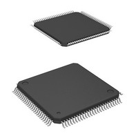
DF2238RTF6 Renesas Electronics America, DF2238RTF6 Datasheet - Page 736

DF2238RTF6
Manufacturer Part Number
DF2238RTF6
Description
MCU 2.2/3V 256K 100-TQFP
Manufacturer
Renesas Electronics America
Series
H8® H8S/2200r
Datasheet
1.DF2238RFA6V.pdf
(1048 pages)
Specifications of DF2238RTF6
Core Processor
H8S/2000
Core Size
16-Bit
Speed
6MHz
Connectivity
I²C, SCI, SmartCard
Peripherals
POR, PWM, WDT
Number Of I /o
72
Program Memory Size
256KB (256K x 8)
Program Memory Type
FLASH
Ram Size
16K x 8
Voltage - Supply (vcc/vdd)
2.2 V ~ 3.6 V
Data Converters
A/D 8x10b; D/A 2x8b
Oscillator Type
Internal
Operating Temperature
-20°C ~ 75°C
Package / Case
100-TQFP, 100-VQFP
Lead Free Status / RoHS Status
Contains lead / RoHS non-compliant
Eeprom Size
-
Other names
HD64F2238RTF6
HD64F2238RTF6
HD64F2238RTF6
Available stocks
Company
Part Number
Manufacturer
Quantity
Price
Company:
Part Number:
DF2238RTF6V
Manufacturer:
Renesas Electronics America
Quantity:
10 000
- Current page: 736 of 1048
- Download datasheet (6Mb)
Section 16 I
16.4.9
The logic levels at the SCL and SDA pins are routed through noise cancelers before being latched
internally. Figure 16.20 shows a block diagram of the noise canceler circuit.
The noise canceler consists of two cascaded latches and a match detector. The SCL (or SDA)
input signal is sampled on the system clock, but is not passed forward to the next circuit unless the
outputs of both latches agree. If they do not agree, the previous value is held.
16.4.10 Initialization of Internal State
The IIC has a function for forcible initialization of its internal state if a deadlock occurs during
communication.
Initialization is executed by (1) setting bits CLR3 to CLR0 in the DDCSWR register or (2)
clearing the ICE bit. For details of settings for bits CLR3 to CLR0, see section 16.3.8, DDC
Switch Register (DDCSWR).
Scope of Initialization: The initialization executed by this function covers the following items:
• TDRE and RDRF internal flags
• Transmit/receive sequencer and internal operating clock counter
• Internal latches for retaining the output state of the SCL and SDA pins (wait, clock, data
Rev. 6.00 Mar. 18, 2010 Page 674 of 982
REJ09B0054-0600
SCL or
SDA input
signal
Sampling
clock
output, etc.)
Noise Canceler
2
C Bus Interface (IIC) (Option)
D
Sampling clock
System clock
period
Latch
Figure 16.20 Block Diagram of Noise Canceler
C
Q
D
Latch
C
Q
detector
Match
Internal
SCL or
SDA
signal
Related parts for DF2238RTF6
Image
Part Number
Description
Manufacturer
Datasheet
Request
R

Part Number:
Description:
CONN SOCKET 2POS 7.92MM WHITE
Manufacturer:
Hirose Electric Co Ltd
Datasheet:

Part Number:
Description:
CONN SOCKET 4POS 7.92MM WHITE
Manufacturer:
Hirose Electric Co Ltd
Datasheet:

Part Number:
Description:
CONN SOCKET 5POS 7.92MM WHITE
Manufacturer:
Hirose Electric Co Ltd
Datasheet:

Part Number:
Description:
CONN SOCKET 3POS 7.92MM WHITE
Manufacturer:
Hirose Electric Co Ltd
Datasheet:

Part Number:
Description:
CONN SOCKET 5POS 7.92MM WHITE
Manufacturer:
Hirose Electric Co Ltd
Datasheet:

Part Number:
Description:
CONN SOCKET 2POS 7.92MM WHITE
Manufacturer:
Hirose Electric Co Ltd
Datasheet:

Part Number:
Description:
CONN SOCKET 3POS 7.92MM WHITE
Manufacturer:
Hirose Electric Co Ltd
Datasheet:

Part Number:
Description:
CONN SOCKET 4POS 7.92MM WHITE
Manufacturer:
Hirose Electric Co Ltd
Datasheet:

Part Number:
Description:
CONN HEADER 2POS 7.92MM R/A TIN
Manufacturer:
Hirose Electric Co Ltd
Datasheet:

Part Number:
Description:
CONN HEADER 4POS 7.92MM R/A TIN
Manufacturer:
Hirose Electric Co Ltd
Datasheet:

Part Number:
Description:
KIT STARTER FOR M16C/29
Manufacturer:
Renesas Electronics America
Datasheet:

Part Number:
Description:
KIT STARTER FOR R8C/2D
Manufacturer:
Renesas Electronics America
Datasheet:

Part Number:
Description:
R0K33062P STARTER KIT
Manufacturer:
Renesas Electronics America
Datasheet:

Part Number:
Description:
KIT STARTER FOR R8C/23 E8A
Manufacturer:
Renesas Electronics America
Datasheet:

Part Number:
Description:
KIT STARTER FOR R8C/25
Manufacturer:
Renesas Electronics America
Datasheet:


