C8051F352 Silicon Laboratories Inc, C8051F352 Datasheet - Page 182
C8051F352
Manufacturer Part Number
C8051F352
Description
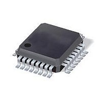
IC 8051 MCU 8K FLASH 32LQFP
Manufacturer
Silicon Laboratories Inc
Series
C8051F35xr
Specifications of C8051F352
Core Processor
8051
Core Size
8-Bit
Speed
50MHz
Connectivity
SMBus (2-Wire/I²C), SPI, UART/USART
Peripherals
POR, PWM, Temp Sensor, WDT
Number Of I /o
17
Program Memory Size
8KB (8K x 8)
Program Memory Type
FLASH
Ram Size
768 x 8
Voltage - Supply (vcc/vdd)
2.7 V ~ 3.6 V
Data Converters
A/D 8x16b; D/A 2x8b
Oscillator Type
Internal
Operating Temperature
-40°C ~ 85°C
Package / Case
32-LQFP
Processor Series
C8051F35x
Core
8051
Data Bus Width
8 bit
Data Ram Size
768 B
Interface Type
I2C, SPI, UART
Maximum Clock Frequency
50 MHz
Number Of Programmable I/os
17
Number Of Timers
4
Operating Supply Voltage
2.7 V to 3.6 V
Maximum Operating Temperature
+ 85 C
Mounting Style
SMD/SMT
Minimum Operating Temperature
- 40 C
On-chip Adc
16 bit
On-chip Dac
8 bit
Lead Free Status / RoHS Status
Contains lead / RoHS non-compliant
Eeprom Size
-
Lead Free Status / Rohs Status
No
Available stocks
Company
Part Number
Manufacturer
Quantity
Price
Company:

Part Number:
C8051F352
Manufacturer:
SILICON
Quantity:
364
Company:
Part Number:
C8051F352
Manufacturer:
Silicon Laboratories Inc
Quantity:
10 000
Company:
Part Number:
C8051F352-GQ
Manufacturer:
SiliconL
Quantity:
3 843
Company:
Part Number:
C8051F352-GQ
Manufacturer:
SILICON
Quantity:
4
Company:
Part Number:
C8051F352-GQ
Manufacturer:
Silicon Laboratories Inc
Quantity:
10 000
Part Number:
C8051F352-GQ
Manufacturer:
SILICON LABS/èٹ¯ç§‘
Quantity:
20 000
Company:
Part Number:
C8051F352-GQR
Manufacturer:
Silicon Laboratories Inc
Quantity:
10 000
Company:
Part Number:
C8051F352-GQR..
Manufacturer:
SILICON
Quantity:
15 000
Company:
Part Number:
C8051F352R
Manufacturer:
Silicon Laboratories Inc
Quantity:
10 000


C8051F350/1/2/3
21.5. Serial Clock Timing
Four combinations of serial clock phase and polarity can be selected using the clock control bits in the
SPI0 Configuration Register (SPI0CFG). The CKPHA bit (SPI0CFG.5) selects one of two clock phases
(edge used to latch the data). The CKPOL bit (SPI0CFG.4) selects between an active-high or active-low
clock. Both master and slave devices must be configured to use the same clock phase and polarity. SPI0
should be disabled (by clearing the SPIEN bit, SPI0CN.0) when changing the clock phase or polarity. The
clock and data line relationships are shown in Figure 21.5.
The SPI0 Clock Rate Register (SPI0CKR) as shown in Figure 21.8 controls the master mode serial clock
frequency. This register is ignored when operating in slave mode. When the SPI is configured as a master,
the maximum data transfer rate (bits/sec) is one-half the system clock frequency or 12.5 MHz, whichever is
slower. When the SPI is configured as a slave, the maximum data transfer rate (bits/sec) for full-duplex
operation is 1/10 the system clock frequency, provided that the master issues SCK, NSS (in 4-wire slave
mode), and the serial input data synchronously with the slave’s system clock. If the master issues SCK,
NSS, and the serial input data asynchronously, the maximum data transfer rate (bits/sec) must be less
than 1/10 the system clock frequency. In the special case where the master only wants to transmit data to
the slave and does not need to receive data from the slave (i.e. half-duplex operation), the SPI slave can
receive data at a maximum data transfer rate (bits/sec) of 1/4 the system clock frequency. This is provided
that the master issues SCK, NSS, and the serial input data synchronously with the slave’s system clock.
21.6. SPI Special Function Registers
SPI0 is accessed and controlled through four special function registers in the system controller: SPI0CN
Control Register, SPI0DAT Data Register, SPI0CFG Configuration Register, and SPI0CKR Clock Rate
Register. The four special function registers related to the operation of the SPI0 Bus are described in the
following figures.
182
SCK
(CKPOL=0, CKPHA=0)
SCK
(CKPOL=0, CKPHA=1)
SCK
(CKPOL=1, CKPHA=0)
SCK
(CKPOL=1, CKPHA=1)
MISO/MOSI
Figure 21.5. Data/Clock Timing Relationship
MSB
Bit 6
Bit 5
Rev. 0.4
Bit 4
Bit 3
Bit 2
Bit 1
Bit 0
Related parts for C8051F352
Image
Part Number
Description
Manufacturer
Datasheet
Request
R

Part Number:
Description:
SMD/C°/SINGLE-ENDED OUTPUT SILICON OSCILLATOR
Manufacturer:
Silicon Laboratories Inc
Part Number:
Description:
Manufacturer:
Silicon Laboratories Inc
Datasheet:
Part Number:
Description:
N/A N/A/SI4010 AES KEYFOB DEMO WITH LCD RX
Manufacturer:
Silicon Laboratories Inc
Datasheet:
Part Number:
Description:
N/A N/A/SI4010 SIMPLIFIED KEY FOB DEMO WITH LED RX
Manufacturer:
Silicon Laboratories Inc
Datasheet:
Part Number:
Description:
N/A/-40 TO 85 OC/EZLINK MODULE; F930/4432 HIGH BAND (REV E/B1)
Manufacturer:
Silicon Laboratories Inc
Part Number:
Description:
EZLink Module; F930/4432 Low Band (rev e/B1)
Manufacturer:
Silicon Laboratories Inc
Part Number:
Description:
I°/4460 10 DBM RADIO TEST CARD 434 MHZ
Manufacturer:
Silicon Laboratories Inc
Part Number:
Description:
I°/4461 14 DBM RADIO TEST CARD 868 MHZ
Manufacturer:
Silicon Laboratories Inc
Part Number:
Description:
I°/4463 20 DBM RFSWITCH RADIO TEST CARD 460 MHZ
Manufacturer:
Silicon Laboratories Inc
Part Number:
Description:
I°/4463 20 DBM RADIO TEST CARD 868 MHZ
Manufacturer:
Silicon Laboratories Inc
Part Number:
Description:
I°/4463 27 DBM RADIO TEST CARD 868 MHZ
Manufacturer:
Silicon Laboratories Inc
Part Number:
Description:
I°/4463 SKYWORKS 30 DBM RADIO TEST CARD 915 MHZ
Manufacturer:
Silicon Laboratories Inc
Part Number:
Description:
N/A N/A/-40 TO 85 OC/4463 RFMD 30 DBM RADIO TEST CARD 915 MHZ
Manufacturer:
Silicon Laboratories Inc
Part Number:
Description:
I°/4463 20 DBM RADIO TEST CARD 169 MHZ
Manufacturer:
Silicon Laboratories Inc