C8051F352 Silicon Laboratories Inc, C8051F352 Datasheet - Page 42
C8051F352
Manufacturer Part Number
C8051F352
Description
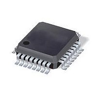
IC 8051 MCU 8K FLASH 32LQFP
Manufacturer
Silicon Laboratories Inc
Series
C8051F35xr
Specifications of C8051F352
Core Processor
8051
Core Size
8-Bit
Speed
50MHz
Connectivity
SMBus (2-Wire/I²C), SPI, UART/USART
Peripherals
POR, PWM, Temp Sensor, WDT
Number Of I /o
17
Program Memory Size
8KB (8K x 8)
Program Memory Type
FLASH
Ram Size
768 x 8
Voltage - Supply (vcc/vdd)
2.7 V ~ 3.6 V
Data Converters
A/D 8x16b; D/A 2x8b
Oscillator Type
Internal
Operating Temperature
-40°C ~ 85°C
Package / Case
32-LQFP
Processor Series
C8051F35x
Core
8051
Data Bus Width
8 bit
Data Ram Size
768 B
Interface Type
I2C, SPI, UART
Maximum Clock Frequency
50 MHz
Number Of Programmable I/os
17
Number Of Timers
4
Operating Supply Voltage
2.7 V to 3.6 V
Maximum Operating Temperature
+ 85 C
Mounting Style
SMD/SMT
Minimum Operating Temperature
- 40 C
On-chip Adc
16 bit
On-chip Dac
8 bit
Lead Free Status / RoHS Status
Contains lead / RoHS non-compliant
Eeprom Size
-
Lead Free Status / Rohs Status
No
Available stocks
Company
Part Number
Manufacturer
Quantity
Price
Company:

Part Number:
C8051F352
Manufacturer:
SILICON
Quantity:
364
Company:
Part Number:
C8051F352
Manufacturer:
Silicon Laboratories Inc
Quantity:
10 000
Company:
Part Number:
C8051F352-GQ
Manufacturer:
SiliconL
Quantity:
3 843
Company:
Part Number:
C8051F352-GQ
Manufacturer:
SILICON
Quantity:
4
Company:
Part Number:
C8051F352-GQ
Manufacturer:
Silicon Laboratories Inc
Quantity:
10 000
Part Number:
C8051F352-GQ
Manufacturer:
SILICON LABS/èٹ¯ç§‘
Quantity:
20 000
Company:
Part Number:
C8051F352-GQR
Manufacturer:
Silicon Laboratories Inc
Quantity:
10 000
Company:
Part Number:
C8051F352-GQR..
Manufacturer:
SILICON
Quantity:
15 000
Company:
Part Number:
C8051F352R
Manufacturer:
Silicon Laboratories Inc
Quantity:
10 000


C8051F350/1/2/3
5.2.
Calibrating the ADC
ADC0 can be calibrated in-system for both gain and offset, using internal or system calibration modes. To
ensure calibration accuracy, offset calibrations must be performed prior to gain calibrations. It is not neces-
sary to perform both internal and system calibrations, as a system calibration will also compensate for any
internal error sources.
Offset calibration is a single-point measurement that sets which input voltage produces a zero at the ADC
output. When performing an offset calibration, any deviation from zero in the measurement is stored in the
offset register. The offset value is subtracted from all conversions as they take place.
Gain calibration is a two-point measurement that sets the slope of the ADC transfer function. When per-
formed, a gain calibration takes only a single measurement, which is assumed to be the desired full-scale
value in the ADC transfer function. The offset calibration value is used as the other point in the gain calibra-
tion measurement, so that a gain factor can be calculated. After offset correction, conversions are multi-
plied by the gain factor.
Calibrations are initiated by writing the ADC System Mode bits (AD0SM) to one of the calibration options.
During a calibration, the AD0CBSY bit is set to ‘1’. Upon completion of a calibration the the AD0SM bits will
return to Idle mode, the AD0CBSY bit will be cleared to ‘0’, the AD0CALC bit will be set to ‘1’, and an ADC
interrupt will be generated. The AD0CALC bit is cleared by clearing the AD0INT flag. Calibration results
are also written to the appropriate calibration registers when the calibration is complete.
5.2.1. Internal Calibration
Internal calibration is performed without requiring a specific voltage on the ADC input pins. Internal calibra-
tions can be performed in three different ways: offset only, gain only, or full (offset and gain). A full internal
calibration consists of an internal offset calibration followed by an internal gain calibration. If offset and gain
calibrations are performed independently, offset calibration must be performed prior to gain calibration.
During an internal offset calibration, the ADC inputs are connected internally to AGND. For an internal gain
calibration, the ADC inputs are connected internally to a full-scale Voltage that is equal to the selected Volt-
age reference divided by the PGA gain.
5.2.2. System Calibration
System calibration is performed using voltages which are applied to the ADC inputs. There are two system
calibration options: offset calibration and gain calibration. For accurate calibration results, offset calibration
must be performed prior to gain calibration. During a system offset calibration, the ADC inputs should be
connected to a “zero” value. During a system gain calibration, the ADC inputs should be connected to the
positive full-scale value for the current PGA gain setting.
5.2.3. Calibration Coefficient Storage
The calibration results for offset and gain are each 24-bits long. The calibration results are stored in SFRs
that are both readable and writeable from software. This enables factory calibrations, as well as manual
modification of the offset and gain parameters. The offset calibration results are stored as a two’s comple-
ment, 24-bit number in the ADC0COH, ADC0COM, and ADC0COL registers. The mapping of the offset
register is shown in Figure 5.3. The gain calibration results are stored as a fixed-point, 24-bit number in the
42
Rev. 0.4
Related parts for C8051F352
Image
Part Number
Description
Manufacturer
Datasheet
Request
R

Part Number:
Description:
SMD/C°/SINGLE-ENDED OUTPUT SILICON OSCILLATOR
Manufacturer:
Silicon Laboratories Inc
Part Number:
Description:
Manufacturer:
Silicon Laboratories Inc
Datasheet:
Part Number:
Description:
N/A N/A/SI4010 AES KEYFOB DEMO WITH LCD RX
Manufacturer:
Silicon Laboratories Inc
Datasheet:
Part Number:
Description:
N/A N/A/SI4010 SIMPLIFIED KEY FOB DEMO WITH LED RX
Manufacturer:
Silicon Laboratories Inc
Datasheet:
Part Number:
Description:
N/A/-40 TO 85 OC/EZLINK MODULE; F930/4432 HIGH BAND (REV E/B1)
Manufacturer:
Silicon Laboratories Inc
Part Number:
Description:
EZLink Module; F930/4432 Low Band (rev e/B1)
Manufacturer:
Silicon Laboratories Inc
Part Number:
Description:
I°/4460 10 DBM RADIO TEST CARD 434 MHZ
Manufacturer:
Silicon Laboratories Inc
Part Number:
Description:
I°/4461 14 DBM RADIO TEST CARD 868 MHZ
Manufacturer:
Silicon Laboratories Inc
Part Number:
Description:
I°/4463 20 DBM RFSWITCH RADIO TEST CARD 460 MHZ
Manufacturer:
Silicon Laboratories Inc
Part Number:
Description:
I°/4463 20 DBM RADIO TEST CARD 868 MHZ
Manufacturer:
Silicon Laboratories Inc
Part Number:
Description:
I°/4463 27 DBM RADIO TEST CARD 868 MHZ
Manufacturer:
Silicon Laboratories Inc
Part Number:
Description:
I°/4463 SKYWORKS 30 DBM RADIO TEST CARD 915 MHZ
Manufacturer:
Silicon Laboratories Inc
Part Number:
Description:
N/A N/A/-40 TO 85 OC/4463 RFMD 30 DBM RADIO TEST CARD 915 MHZ
Manufacturer:
Silicon Laboratories Inc
Part Number:
Description:
I°/4463 20 DBM RADIO TEST CARD 169 MHZ
Manufacturer:
Silicon Laboratories Inc