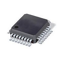
C8051F352 Silicon Laboratories Inc, C8051F352 Datasheet - Page 184

C8051F352
Manufacturer Part Number
C8051F352
Description
IC 8051 MCU 8K FLASH 32LQFP
Manufacturer
Silicon Laboratories Inc
Series
C8051F35xr
Specifications of C8051F352
Core Processor
8051
Core Size
8-Bit
Speed
50MHz
Connectivity
SMBus (2-Wire/I²C), SPI, UART/USART
Peripherals
POR, PWM, Temp Sensor, WDT
Number Of I /o
17
Program Memory Size
8KB (8K x 8)
Program Memory Type
FLASH
Ram Size
768 x 8
Voltage - Supply (vcc/vdd)
2.7 V ~ 3.6 V
Data Converters
A/D 8x16b; D/A 2x8b
Oscillator Type
Internal
Operating Temperature
-40°C ~ 85°C
Package / Case
32-LQFP
Processor Series
C8051F35x
Core
8051
Data Bus Width
8 bit
Data Ram Size
768 B
Interface Type
I2C, SPI, UART
Maximum Clock Frequency
50 MHz
Number Of Programmable I/os
17
Number Of Timers
4
Operating Supply Voltage
2.7 V to 3.6 V
Maximum Operating Temperature
+ 85 C
Mounting Style
SMD/SMT
Minimum Operating Temperature
- 40 C
On-chip Adc
16 bit
On-chip Dac
8 bit
Lead Free Status / RoHS Status
Contains lead / RoHS non-compliant
Eeprom Size
-
Lead Free Status / Rohs Status
No
Available stocks
Company
Part Number
Manufacturer
Quantity
Price
Company:
Part Number:
C8051F352
Manufacturer:
SILICON
Quantity:
364
Company:
Part Number:
C8051F352
Manufacturer:
Silicon Laboratories Inc
Quantity:
10 000
Company:
Part Number:
C8051F352-GQ
Manufacturer:
SiliconL
Quantity:
3 843
Company:
Part Number:
C8051F352-GQ
Manufacturer:
SILICON
Quantity:
4
Company:
Part Number:
C8051F352-GQ
Manufacturer:
Silicon Laboratories Inc
Quantity:
10 000
Part Number:
C8051F352-GQ
Manufacturer:
SILICON LABS/èٹ¯ç§‘
Quantity:
20 000
Company:
Part Number:
C8051F352-GQR
Manufacturer:
Silicon Laboratories Inc
Quantity:
10 000
Company:
Part Number:
C8051F352-GQR..
Manufacturer:
SILICON
Quantity:
15 000
Company:
Part Number:
C8051F352R
Manufacturer:
Silicon Laboratories Inc
Quantity:
10 000
C8051F350/1/2/3
184
Bit 7:
Bit 6:
Bit 5:
Bit 4:
Bits 3-2: NSSMD1-NSSMD0: Slave Select Mode.
Bit 1:
Bit 0:
SPIF
R/W
Bit7
SPIF: SPI0 Interrupt Flag.
This bit is set to logic 1 by hardware at the end of a data transfer. If interrupts are enabled,
setting this bit causes the CPU to vector to the SPI0 interrupt service routine. This bit is not
automatically cleared by hardware. It must be cleared by software.
WCOL: Write Collision Flag.
This bit is set to logic 1 by hardware (and generates a SPI0 interrupt) to indicate a write to
the SPI0 data register was attempted while a data transfer was in progress. This bit is not
automatically cleared by hardware. It must be cleared by software.
MODF: Mode Fault Flag.
This bit is set to logic 1 by hardware (and generates a SPI0 interrupt) when a master mode
collision is detected (NSS is low, MSTEN = 1, and NSSMD[1:0] = 01). This bit is not auto-
matically cleared by hardware. It must be cleared by software.
RXOVRN: Receive Overrun Flag (Slave Mode only).
This bit is set to logic 1 by hardware (and generates a SPI0 interrupt) when the receive
buffer still holds unread data from a previous transfer and the last bit of the current transfer is
shifted into the SPI0 shift register. This bit is not automatically cleared by hardware. It must
be cleared by software.
Selects between the following NSS operation modes:
(See
Slave Mode Operation” on page
00: 3-Wire Slave or 3-wire Master Mode. NSS signal is not routed to a port pin.
01: 4-Wire Slave or Multi-Master Mode (Default). NSS is always an input to the device.
1x: 4-Wire Single-Master Mode. NSS signal is mapped as an output from the device and will
assume the value of NSSMD0.
TXBMT: Transmit Buffer Empty.
This bit will be set to logic 0 when new data has been written to the transmit buffer. When
data in the transmit buffer is transferred to the SPI shift register, this bit will be set to logic 1,
indicating that it is safe to write a new byte to the transmit buffer.
SPIEN: SPI0 Enable.
This bit enables/disables the SPI.
0: SPI disabled.
1: SPI enabled.
WCOL
R/W
Bit6
Section “21.2. SPI0 Master Mode Operation” on page 179
Figure 21.7. SPI0CN: SPI0 Control Register
MODF
R/W
Bit5
RXOVRN NSSMD1 NSSMD0
R/W
Bit4
181).
Rev. 0.4
R/W
Bit3
R/W
Bit2
TXBMT
Bit1
R
and
Section “21.3. SPI0
SFR Address: 0xF8
SPIEN
R/W
Bit0
Addressable
Reset Value
00000110
Bit


