C8051F352 Silicon Laboratories Inc, C8051F352 Datasheet - Page 5
C8051F352
Manufacturer Part Number
C8051F352
Description
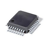
IC 8051 MCU 8K FLASH 32LQFP
Manufacturer
Silicon Laboratories Inc
Series
C8051F35xr
Specifications of C8051F352
Core Processor
8051
Core Size
8-Bit
Speed
50MHz
Connectivity
SMBus (2-Wire/I²C), SPI, UART/USART
Peripherals
POR, PWM, Temp Sensor, WDT
Number Of I /o
17
Program Memory Size
8KB (8K x 8)
Program Memory Type
FLASH
Ram Size
768 x 8
Voltage - Supply (vcc/vdd)
2.7 V ~ 3.6 V
Data Converters
A/D 8x16b; D/A 2x8b
Oscillator Type
Internal
Operating Temperature
-40°C ~ 85°C
Package / Case
32-LQFP
Processor Series
C8051F35x
Core
8051
Data Bus Width
8 bit
Data Ram Size
768 B
Interface Type
I2C, SPI, UART
Maximum Clock Frequency
50 MHz
Number Of Programmable I/os
17
Number Of Timers
4
Operating Supply Voltage
2.7 V to 3.6 V
Maximum Operating Temperature
+ 85 C
Mounting Style
SMD/SMT
Minimum Operating Temperature
- 40 C
On-chip Adc
16 bit
On-chip Dac
8 bit
Lead Free Status / RoHS Status
Contains lead / RoHS non-compliant
Eeprom Size
-
Lead Free Status / Rohs Status
No
Available stocks
Company
Part Number
Manufacturer
Quantity
Price
Company:

Part Number:
C8051F352
Manufacturer:
SILICON
Quantity:
364
Company:
Part Number:
C8051F352
Manufacturer:
Silicon Laboratories Inc
Quantity:
10 000
Company:
Part Number:
C8051F352-GQ
Manufacturer:
SiliconL
Quantity:
3 843
Company:
Part Number:
C8051F352-GQ
Manufacturer:
SILICON
Quantity:
4
Company:
Part Number:
C8051F352-GQ
Manufacturer:
Silicon Laboratories Inc
Quantity:
10 000
Part Number:
C8051F352-GQ
Manufacturer:
SILICON LABS/èٹ¯ç§‘
Quantity:
20 000
Company:
Part Number:
C8051F352-GQR
Manufacturer:
Silicon Laboratories Inc
Quantity:
10 000
Company:
Part Number:
C8051F352-GQR..
Manufacturer:
SILICON
Quantity:
15 000
Company:
Part Number:
C8051F352R
Manufacturer:
Silicon Laboratories Inc
Quantity:
10 000


18. Port Input/Output.................................................................................................. 133
19. SMBus ................................................................................................................... 147
20. UART0.................................................................................................................... 167
21. Serial Peripheral Interface (SPI0) ........................................................................ 177
17.2.External Oscillator Drive Circuit...................................................................... 127
17.3.Clock Multiplier ............................................................................................... 130
17.4.System Clock Selection.................................................................................. 131
18.1.Priority Crossbar Decoder .............................................................................. 135
18.2.Port I/O Initialization ....................................................................................... 137
18.3.General Purpose Port I/O ............................................................................... 140
19.1.Supporting Documents ................................................................................... 148
19.2.SMBus Configuration...................................................................................... 148
19.3.SMBus Operation ........................................................................................... 149
19.4.Using the SMBus............................................................................................ 151
19.5.SMBus Transfer Modes.................................................................................. 159
19.6.SMBus Status Decoding................................................................................. 163
20.1.Enhanced Baud Rate Generation................................................................... 168
20.2.Operational Modes ......................................................................................... 169
20.3.Multiprocessor Communications .................................................................... 171
21.1.Signal Descriptions......................................................................................... 178
21.2.SPI0 Master Mode Operation ......................................................................... 179
21.3.SPI0 Slave Mode Operation ........................................................................... 181
21.4.SPI0 Interrupt Sources ................................................................................... 181
21.5.Serial Clock Timing......................................................................................... 182
17.2.1.Clocking Timers Directly Through the External Oscillator...................... 127
17.2.2.External Crystal Example....................................................................... 127
17.2.3.External RC Example............................................................................. 128
17.2.4.External Capacitor Example................................................................... 128
19.3.1.Arbitration............................................................................................... 149
19.3.2.Clock Low Extension.............................................................................. 150
19.3.3.SCL Low Timeout................................................................................... 150
19.3.4.SCL High (SMBus Free) Timeout .......................................................... 150
19.4.1.SMBus Configuration Register............................................................... 152
19.4.2.SMB0CN Control Register ..................................................................... 155
19.4.3.Data Register ......................................................................................... 158
19.5.1.Master Transmitter Mode ....................................................................... 159
19.5.2.Master Receiver Mode ........................................................................... 160
19.5.3.Slave Receiver Mode ............................................................................. 161
19.5.4.Slave Transmitter Mode ......................................................................... 162
20.2.1.8-Bit UART ............................................................................................. 169
20.2.2.9-Bit UART ............................................................................................. 170
21.1.1.Master Out, Slave In (MOSI).................................................................. 178
21.1.2.Master In, Slave Out (MISO).................................................................. 178
21.1.3.Serial Clock (SCK) ................................................................................. 178
21.1.4.Slave Select (NSS) ................................................................................ 178
Rev. 0.4
C8051F350/1/2/3
5
Related parts for C8051F352
Image
Part Number
Description
Manufacturer
Datasheet
Request
R

Part Number:
Description:
SMD/C°/SINGLE-ENDED OUTPUT SILICON OSCILLATOR
Manufacturer:
Silicon Laboratories Inc
Part Number:
Description:
Manufacturer:
Silicon Laboratories Inc
Datasheet:
Part Number:
Description:
N/A N/A/SI4010 AES KEYFOB DEMO WITH LCD RX
Manufacturer:
Silicon Laboratories Inc
Datasheet:
Part Number:
Description:
N/A N/A/SI4010 SIMPLIFIED KEY FOB DEMO WITH LED RX
Manufacturer:
Silicon Laboratories Inc
Datasheet:
Part Number:
Description:
N/A/-40 TO 85 OC/EZLINK MODULE; F930/4432 HIGH BAND (REV E/B1)
Manufacturer:
Silicon Laboratories Inc
Part Number:
Description:
EZLink Module; F930/4432 Low Band (rev e/B1)
Manufacturer:
Silicon Laboratories Inc
Part Number:
Description:
I°/4460 10 DBM RADIO TEST CARD 434 MHZ
Manufacturer:
Silicon Laboratories Inc
Part Number:
Description:
I°/4461 14 DBM RADIO TEST CARD 868 MHZ
Manufacturer:
Silicon Laboratories Inc
Part Number:
Description:
I°/4463 20 DBM RFSWITCH RADIO TEST CARD 460 MHZ
Manufacturer:
Silicon Laboratories Inc
Part Number:
Description:
I°/4463 20 DBM RADIO TEST CARD 868 MHZ
Manufacturer:
Silicon Laboratories Inc
Part Number:
Description:
I°/4463 27 DBM RADIO TEST CARD 868 MHZ
Manufacturer:
Silicon Laboratories Inc
Part Number:
Description:
I°/4463 SKYWORKS 30 DBM RADIO TEST CARD 915 MHZ
Manufacturer:
Silicon Laboratories Inc
Part Number:
Description:
N/A N/A/-40 TO 85 OC/4463 RFMD 30 DBM RADIO TEST CARD 915 MHZ
Manufacturer:
Silicon Laboratories Inc
Part Number:
Description:
I°/4463 20 DBM RADIO TEST CARD 169 MHZ
Manufacturer:
Silicon Laboratories Inc