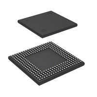
HD6417750SBP200 Renesas Electronics America, HD6417750SBP200 Datasheet - Page 373

HD6417750SBP200
Manufacturer Part Number
HD6417750SBP200
Description
IC SUPERH MPU ROMLESS 256BGA
Manufacturer
Renesas Electronics America
Series
SuperH® SH7750r
Datasheet
1.D6417750RBP240DV.pdf
(1164 pages)
Specifications of HD6417750SBP200
Core Processor
SH-4
Core Size
32-Bit
Speed
200MHz
Connectivity
EBI/EMI, FIFO, SCI, SmartCard
Peripherals
DMA, POR, WDT
Number Of I /o
28
Program Memory Type
ROMless
Ram Size
24K x 8
Voltage - Supply (vcc/vdd)
1.8 V ~ 2.07 V
Oscillator Type
External
Operating Temperature
-20°C ~ 75°C
Package / Case
256-BGA
Lead Free Status / RoHS Status
Contains lead / RoHS non-compliant
Eeprom Size
-
Program Memory Size
-
Data Converters
-
Available stocks
Company
Part Number
Manufacturer
Quantity
Price
Part Number:
HD6417750SBP200
Manufacturer:
RENESAS/瑞萨
Quantity:
20 000
- Current page: 373 of 1164
- Download datasheet (7Mb)
10.1
The on-chip oscillation circuits comprise a clock pulse generator (CPG) and a watchdog timer
(WDT).
The CPG generates the clocks supplied inside the processor and performs power-down mode
control.
The WDT is a single-channel timer used to count the clock stabilization time when exiting standby
mode or the frequency is changed. It can be used as a normal watchdog timer or an interval timer.
10.1.1
The CPG has the following features:
• Three clocks
• Six clock modes
• Frequency change function
• PLL on/off control
• Power-down mode control
The CPG can generate the CPU clock (Ick) used by the CPU, FPU, caches, and TLB, the
peripheral module clock (Pck) used by the peripheral modules, and the bus clock (Bck) used
by the external bus interface.
Any of six clock operating modes can be selected, with different combinations of CPU clock,
bus clock, and peripheral module clock division ratios after a power-on reset.
PLL (phase-locked loop) circuits and a frequency divider in the CPG enable the CPU clock,
bus clock, and peripheral module clock frequencies to be changed independently. Frequency
changes are performed by software in accordance with the settings in the frequency control
register (FRQCR).
Power consumption can be reduced by stopping the PLL circuits during low-frequency
operation.
It is possible to stop the clock in sleep mode and standby mode, and to stop specific modules
with the module standby function.
Features
Overview
Section 10 Clock Oscillation Circuits
Rev.7.00 Oct. 10, 2008 Page 287 of 1074
Section 10 Clock Oscillation Circuits
REJ09B0366-0700
Related parts for HD6417750SBP200
Image
Part Number
Description
Manufacturer
Datasheet
Request
R

Part Number:
Description:
KIT STARTER FOR M16C/29
Manufacturer:
Renesas Electronics America
Datasheet:

Part Number:
Description:
KIT STARTER FOR R8C/2D
Manufacturer:
Renesas Electronics America
Datasheet:

Part Number:
Description:
R0K33062P STARTER KIT
Manufacturer:
Renesas Electronics America
Datasheet:

Part Number:
Description:
KIT STARTER FOR R8C/23 E8A
Manufacturer:
Renesas Electronics America
Datasheet:

Part Number:
Description:
KIT STARTER FOR R8C/25
Manufacturer:
Renesas Electronics America
Datasheet:

Part Number:
Description:
KIT STARTER H8S2456 SHARPE DSPLY
Manufacturer:
Renesas Electronics America
Datasheet:

Part Number:
Description:
KIT STARTER FOR R8C38C
Manufacturer:
Renesas Electronics America
Datasheet:

Part Number:
Description:
KIT STARTER FOR R8C35C
Manufacturer:
Renesas Electronics America
Datasheet:

Part Number:
Description:
KIT STARTER FOR R8CL3AC+LCD APPS
Manufacturer:
Renesas Electronics America
Datasheet:

Part Number:
Description:
KIT STARTER FOR RX610
Manufacturer:
Renesas Electronics America
Datasheet:

Part Number:
Description:
KIT STARTER FOR R32C/118
Manufacturer:
Renesas Electronics America
Datasheet:

Part Number:
Description:
KIT DEV RSK-R8C/26-29
Manufacturer:
Renesas Electronics America
Datasheet:

Part Number:
Description:
KIT STARTER FOR SH7124
Manufacturer:
Renesas Electronics America
Datasheet:

Part Number:
Description:
KIT STARTER FOR H8SX/1622
Manufacturer:
Renesas Electronics America
Datasheet:

Part Number:
Description:
KIT DEV FOR SH7203
Manufacturer:
Renesas Electronics America
Datasheet:


