HD6417750SBP200 Renesas Electronics America, HD6417750SBP200 Datasheet - Page 641
HD6417750SBP200
Manufacturer Part Number
HD6417750SBP200
Description
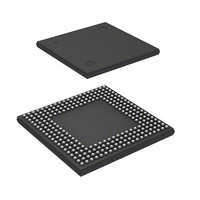
IC SUPERH MPU ROMLESS 256BGA
Manufacturer
Renesas Electronics America
Series
SuperH® SH7750r
Datasheet
1.D6417750RBP240DV.pdf
(1164 pages)
Specifications of HD6417750SBP200
Core Processor
SH-4
Core Size
32-Bit
Speed
200MHz
Connectivity
EBI/EMI, FIFO, SCI, SmartCard
Peripherals
DMA, POR, WDT
Number Of I /o
28
Program Memory Type
ROMless
Ram Size
24K x 8
Voltage - Supply (vcc/vdd)
1.8 V ~ 2.07 V
Oscillator Type
External
Operating Temperature
-20°C ~ 75°C
Package / Case
256-BGA
Lead Free Status / RoHS Status
Contains lead / RoHS non-compliant
Eeprom Size
-
Program Memory Size
-
Data Converters
-
Available stocks
Company
Part Number
Manufacturer
Quantity
Price

Part Number:
HD6417750SBP200
Manufacturer:
RENESAS/瑞萨
Quantity:
20 000


14.2.4
Note: The TE bit can only be written with 0 after being read as 1, to clear the flag.
DMA channel control registers 0–3 (CHCR0–CHCR3) are 32-bit readable/writable registers that
specify the operating mode, transfer method, etc., for each channel. Bits 31–28 and 27–24 indicate
the source address and destination address, respectively; these settings are only valid when the
transfer involves the CS5 or CS6 space and the relevant space has been specified as a PCMCIA
interface space. In other cases, these bits should be cleared to 0. For details of the PCMCIA
interface, see section 13.3.7, PCMCIA Interface, in section 13, Bus State Controller (BSC).
In DDT mode, CHCR0 is set according to the DTR format. (The following settings are fixed:
CHCR0 [31:24] = 0, [18:16] = 0, [15:14] = 01, [13:12] = 01, [2] = 0, [1] = 0, [0] = 1)
Bits 18 and 16 are not present in CHCR2 and CHCR3. In CHCR2 and CHCR3, these bits cannot
be modified (a write value of 0 should always be used) and are always read as 0.
Initial value:
Initial value:
Initial value:
Initial value:
The RL, AM, AL, and DS bits may be absent, depending on the channel.
DMA Channel Control Registers 0–3 (CHCR0–CHCR3)
R/W:
R/W:
R/W:
R/W:
Bit:
Bit:
Bit:
Bit:
SSA2
DM1
R/W
R/W
R/W
TM
31
23
15
—
R
0
0
0
7
0
SSA1
DM0
R/W
R/W
R/W
TS2
30
22
14
—
R
0
0
0
6
0
SSA0
SM1
R/W
R/W
R/W
TS1
29
21
13
—
R
0
0
0
5
0
Section 14 Direct Memory Access Controller (DMAC)
STC
SM0
R/W
R/W
R/W
TS0
28
20
12
—
R
0
0
0
4
0
Rev.7.00 Oct. 10, 2008 Page 555 of 1074
DSA2
R/W
R/W
RS3
R/W
DS
27
19
11
—
R
0
0
0
3
0
DSA1
(R/W)
R/W
RS2
R/W
R/W
RL
26
18
10
IE
0
0
0
2
0
REJ09B0366-0700
DSA0
R/(W)
R/W
R/W
RS1
R/W
AM
TE
25
17
0
0
9
0
1
0
(R/W)
DTC
RS0
R/W
R/W
R/W
DE
AL
24
16
0
0
8
0
0
0
Related parts for HD6417750SBP200
Image
Part Number
Description
Manufacturer
Datasheet
Request
R

Part Number:
Description:
KIT STARTER FOR M16C/29
Manufacturer:
Renesas Electronics America
Datasheet:

Part Number:
Description:
KIT STARTER FOR R8C/2D
Manufacturer:
Renesas Electronics America
Datasheet:

Part Number:
Description:
R0K33062P STARTER KIT
Manufacturer:
Renesas Electronics America
Datasheet:

Part Number:
Description:
KIT STARTER FOR R8C/23 E8A
Manufacturer:
Renesas Electronics America
Datasheet:

Part Number:
Description:
KIT STARTER FOR R8C/25
Manufacturer:
Renesas Electronics America
Datasheet:

Part Number:
Description:
KIT STARTER H8S2456 SHARPE DSPLY
Manufacturer:
Renesas Electronics America
Datasheet:

Part Number:
Description:
KIT STARTER FOR R8C38C
Manufacturer:
Renesas Electronics America
Datasheet:

Part Number:
Description:
KIT STARTER FOR R8C35C
Manufacturer:
Renesas Electronics America
Datasheet:

Part Number:
Description:
KIT STARTER FOR R8CL3AC+LCD APPS
Manufacturer:
Renesas Electronics America
Datasheet:
Part Number:
Description:
KIT STARTER FOR RX610
Manufacturer:
Renesas Electronics America
Datasheet:

Part Number:
Description:
KIT STARTER FOR R32C/118
Manufacturer:
Renesas Electronics America
Datasheet:

Part Number:
Description:
KIT DEV RSK-R8C/26-29
Manufacturer:
Renesas Electronics America
Datasheet:

Part Number:
Description:
KIT STARTER FOR SH7124
Manufacturer:
Renesas Electronics America
Datasheet:

Part Number:
Description:
KIT STARTER FOR H8SX/1622
Manufacturer:
Renesas Electronics America
Datasheet:

Part Number:
Description:
KIT DEV FOR SH7203
Manufacturer:
Renesas Electronics America
Datasheet: