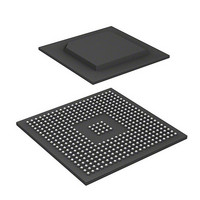
R8A77850BDBGV#RD0Z Renesas Electronics America, R8A77850BDBGV#RD0Z Datasheet - Page 1158

R8A77850BDBGV#RD0Z
Manufacturer Part Number
R8A77850BDBGV#RD0Z
Description
IC SUPERH MPU ROMLESS 436BGA
Manufacturer
Renesas Electronics America
Series
SuperH® SH7780r
Datasheet
1.R8A77850AADBGV.pdf
(1694 pages)
Specifications of R8A77850BDBGV#RD0Z
Core Processor
SH-4A
Core Size
32-Bit
Speed
600MHz
Connectivity
Audio Codec, MMC, Serial Sound, SCI, SIO, SPI, SSI
Peripherals
DMA, POR, WDT
Number Of I /o
108
Program Memory Type
ROMless
Ram Size
8K x 8
Voltage - Supply (vcc/vdd)
1 V ~ 1.2 V
Oscillator Type
External
Operating Temperature
-40°C ~ 85°C
Package / Case
436-BGA
Lead Free Status / RoHS Status
Lead free / RoHS Compliant
Eeprom Size
-
Program Memory Size
-
Data Converters
-
Available stocks
Company
Part Number
Manufacturer
Quantity
Price
- Current page: 1158 of 1694
- Download datasheet (9Mb)
22. Serial I/O with FIFO (SIOF)
22.3.13 Control Data Assign Register (SICDAR)
SICDAR is a 16-bit readable/writable register that specifies the position of the control data in a
frame. SICDAR can be specified only when the FL bits in SIMDR are set to 1xxx (x: don't care.).
Rev.1.00 Jan. 10, 2008 Page 1126 of 1658
REJ09B0261-0100
Initial value:
Bit
15
14 to 12 ⎯
11 to 8
7
6 to 4
R/W:
BIt:
Bit Name
CD0E
CD0A[3:0]
CD1E
⎯
CD0E
R/W
15
0
14
—
R
0
13
—
R
0
Initial
Value
0
All 0
0000
0
All 0
12
—
R
0
R/W
R/W
R/W
R
R/W
R/W
R
11
0
R/W
CD0
10
0
A[3:0]
Description
Control Channel 0 Data Enable
0: Disables transmission and reception of control
1: Enables transmission and reception of control
Reserved
These bits are always read as 0. The write value should
always be 0.
Control Channel 0 Data Assigns 3 to 0
These bits specify the position of control channel 0 data
in a receive or transmit frame as B'0000 (0) to B'1110
(14).
1111: Setting prohibited
•
•
Control Channel 1 Data Enable
0: Disables transmission and reception of control
1: Enables transmission and reception of control
Reserved
These bits are always read as 0. The write value should
always be 0.
R/W
channel 0 data
channel 0 data
channel 1 data
channel 1 data
9
0
Transmit data for the control channel 0 data is
specified in the SITD0 bit in SITCR.
Receive data for the control channel 0 data is stored
in the SIRD0 bit in SIRCR.
R/W
8
0
CD1E
R/W
7
0
—
R
6
0
—
R
5
0
—
R
4
0
R/W
3
0
R/W
CD1
2
0
A[3:0]
R/W
1
0
R/W
0
0
Related parts for R8A77850BDBGV#RD0Z
Image
Part Number
Description
Manufacturer
Datasheet
Request
R

Part Number:
Description:
KIT STARTER FOR M16C/29
Manufacturer:
Renesas Electronics America
Datasheet:

Part Number:
Description:
KIT STARTER FOR R8C/2D
Manufacturer:
Renesas Electronics America
Datasheet:

Part Number:
Description:
R0K33062P STARTER KIT
Manufacturer:
Renesas Electronics America
Datasheet:

Part Number:
Description:
KIT STARTER FOR R8C/23 E8A
Manufacturer:
Renesas Electronics America
Datasheet:

Part Number:
Description:
KIT STARTER FOR R8C/25
Manufacturer:
Renesas Electronics America
Datasheet:

Part Number:
Description:
KIT STARTER H8S2456 SHARPE DSPLY
Manufacturer:
Renesas Electronics America
Datasheet:

Part Number:
Description:
KIT STARTER FOR R8C38C
Manufacturer:
Renesas Electronics America
Datasheet:

Part Number:
Description:
KIT STARTER FOR R8C35C
Manufacturer:
Renesas Electronics America
Datasheet:

Part Number:
Description:
KIT STARTER FOR R8CL3AC+LCD APPS
Manufacturer:
Renesas Electronics America
Datasheet:

Part Number:
Description:
KIT STARTER FOR RX610
Manufacturer:
Renesas Electronics America
Datasheet:

Part Number:
Description:
KIT STARTER FOR R32C/118
Manufacturer:
Renesas Electronics America
Datasheet:

Part Number:
Description:
KIT DEV RSK-R8C/26-29
Manufacturer:
Renesas Electronics America
Datasheet:

Part Number:
Description:
KIT STARTER FOR SH7124
Manufacturer:
Renesas Electronics America
Datasheet:

Part Number:
Description:
KIT STARTER FOR H8SX/1622
Manufacturer:
Renesas Electronics America
Datasheet:

Part Number:
Description:
KIT DEV FOR SH7203
Manufacturer:
Renesas Electronics America
Datasheet:


