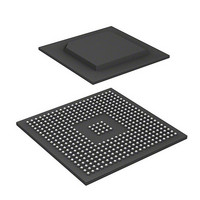
R8A77850BDBGV#RD0Z Renesas Electronics America, R8A77850BDBGV#RD0Z Datasheet - Page 419

R8A77850BDBGV#RD0Z
Manufacturer Part Number
R8A77850BDBGV#RD0Z
Description
IC SUPERH MPU ROMLESS 436BGA
Manufacturer
Renesas Electronics America
Series
SuperH® SH7780r
Datasheet
1.R8A77850AADBGV.pdf
(1694 pages)
Specifications of R8A77850BDBGV#RD0Z
Core Processor
SH-4A
Core Size
32-Bit
Speed
600MHz
Connectivity
Audio Codec, MMC, Serial Sound, SCI, SIO, SPI, SSI
Peripherals
DMA, POR, WDT
Number Of I /o
108
Program Memory Type
ROMless
Ram Size
8K x 8
Voltage - Supply (vcc/vdd)
1 V ~ 1.2 V
Oscillator Type
External
Operating Temperature
-40°C ~ 85°C
Package / Case
436-BGA
Lead Free Status / RoHS Status
Lead free / RoHS Compliant
Eeprom Size
-
Program Memory Size
-
Data Converters
-
Available stocks
Company
Part Number
Manufacturer
Quantity
Price
- Current page: 419 of 1694
- Download datasheet (9Mb)
11.5
11.5.1
This LSI supports both big and little endian modes. In big endian mode, the most significant byte
(MSByte) in a string of byte data is stored at address 0, and in little endian mode, the least
significant byte (LSByte) in a string of byte data is stored at address 0. The mode is specified by
the external pin (MODE8 pin) at a power-on reset by the PRESET pin. At a power-on reset by the
PRESET pin, big endian mode is specified when the MODE8 pin is low, and little endian mode is
specified when the MODE8 pin is high.
The data bus width can be selected from 8, 16 and 32 bits for the normal memory interface. For
the PCMCIA interface, a data bus width of 8 or 16 bits can be selected. Data is aligned according
to the data bus width and endian mode of each device. Therefore, when the data bus width is
smaller than the access size, multiple bus cycles are automatically generated to reach the access
size. In this case, access is performed by incrementing the addresses corresponding to the bus
width. For example, when a longword access is performed in the area with an 8-bit width with the
SRAM interface, each address is incremented by one, and accesses are performed four times. In
the 32-byte transfer, a total of 32-byte data is continuously transferred according to the specified
bus width. The first access is performed on the data for which there was an access request, and the
remaining accesses are performed on the subsequent data up to the nearest 32-byte boundary in a
wraparound manner. The bus is not released during these transfers. This LSI automatically aligns
data and changes the data length between interfaces.
In an 8- or 16-byte transfer, the LBSC executes the 4-byte accesses twice and four times
respectively.
Tables 11.6 to 11.15 show the relationship between the device data width, endian mode and access
size.
Data structure
Byte
Word
Longword
Operation
Endian/Access Size and Data Alignment
MSB
MSB
MSB
Data 31 to 24
Data 15 to 8
Data 7 to 0
LSB
LSB
Data 23 to 16
Data 7 to 0
LSB
Rev.1.00 Jan. 10, 2008 Page 387 of 1658
Data 15 to 8
11. Local Bus State Controller (LBSC)
Data 7 to 0
REJ09B0261-0100
LSB
Related parts for R8A77850BDBGV#RD0Z
Image
Part Number
Description
Manufacturer
Datasheet
Request
R

Part Number:
Description:
KIT STARTER FOR M16C/29
Manufacturer:
Renesas Electronics America
Datasheet:

Part Number:
Description:
KIT STARTER FOR R8C/2D
Manufacturer:
Renesas Electronics America
Datasheet:

Part Number:
Description:
R0K33062P STARTER KIT
Manufacturer:
Renesas Electronics America
Datasheet:

Part Number:
Description:
KIT STARTER FOR R8C/23 E8A
Manufacturer:
Renesas Electronics America
Datasheet:

Part Number:
Description:
KIT STARTER FOR R8C/25
Manufacturer:
Renesas Electronics America
Datasheet:

Part Number:
Description:
KIT STARTER H8S2456 SHARPE DSPLY
Manufacturer:
Renesas Electronics America
Datasheet:

Part Number:
Description:
KIT STARTER FOR R8C38C
Manufacturer:
Renesas Electronics America
Datasheet:

Part Number:
Description:
KIT STARTER FOR R8C35C
Manufacturer:
Renesas Electronics America
Datasheet:

Part Number:
Description:
KIT STARTER FOR R8CL3AC+LCD APPS
Manufacturer:
Renesas Electronics America
Datasheet:

Part Number:
Description:
KIT STARTER FOR RX610
Manufacturer:
Renesas Electronics America
Datasheet:

Part Number:
Description:
KIT STARTER FOR R32C/118
Manufacturer:
Renesas Electronics America
Datasheet:

Part Number:
Description:
KIT DEV RSK-R8C/26-29
Manufacturer:
Renesas Electronics America
Datasheet:

Part Number:
Description:
KIT STARTER FOR SH7124
Manufacturer:
Renesas Electronics America
Datasheet:

Part Number:
Description:
KIT STARTER FOR H8SX/1622
Manufacturer:
Renesas Electronics America
Datasheet:

Part Number:
Description:
KIT DEV FOR SH7203
Manufacturer:
Renesas Electronics America
Datasheet:


