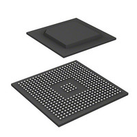
R8A77850BDBGV#RD0Z Renesas Electronics America, R8A77850BDBGV#RD0Z Datasheet - Page 576

R8A77850BDBGV#RD0Z
Manufacturer Part Number
R8A77850BDBGV#RD0Z
Description
IC SUPERH MPU ROMLESS 436BGA
Manufacturer
Renesas Electronics America
Series
SuperH® SH7780r
Datasheet
1.R8A77850AADBGV.pdf
(1694 pages)
Specifications of R8A77850BDBGV#RD0Z
Core Processor
SH-4A
Core Size
32-Bit
Speed
600MHz
Connectivity
Audio Codec, MMC, Serial Sound, SCI, SIO, SPI, SSI
Peripherals
DMA, POR, WDT
Number Of I /o
108
Program Memory Type
ROMless
Ram Size
8K x 8
Voltage - Supply (vcc/vdd)
1 V ~ 1.2 V
Oscillator Type
External
Operating Temperature
-40°C ~ 85°C
Package / Case
436-BGA
Lead Free Status / RoHS Status
Lead free / RoHS Compliant
Eeprom Size
-
Program Memory Size
-
Data Converters
-
Available stocks
Company
Part Number
Manufacturer
Quantity
Price
- Current page: 576 of 1694
- Download datasheet (9Mb)
12. DDR2-SDRAM Interface (DBSC2)
12.5.8
The DDR2-SDRAM specifications limit the number of banks in an 8-bank product which can be
activated simultaneously. Control must be executed so that the number of activated banks never
exceeds four banks. Hence the DBSC2 handles (BA2,BA1,BA0) = (1,X,Y) and (0,X,Y) as access
to the same banks. Through this handling, no more than four banks can be activated
simultaneously. As an operation example, consider a case in which the page corresponding to
bank (BA2,BA1,BA0) = (0,0,0) is opened, and then access of (BA2,BA1,BA0) = (1,0,0) occurs.
After using a PRE command to close the page of the bank corresponding to (BA2,BA1,BA0) =
(0,0,0), the DBSC2 issues an ACT command for the bank corresponding to (BA2,BA1,BA0) =
(1,0,0) to open the page, and accesses the memory. Because the DBSC2 executes the above
control, if a program which is activated simultaneously is placed in an address area such that
(BA2,BA1,BA0) = (1,X,Y) and (0,X,Y), frequent page misses may result.
12.5.9
The following should be noted when having the DBSC2 output an ODT control signal to the
SDRAM.
• When an ODT control signal is output to the SDRAM, a CAS latency of at least four DDR
• When the ODT control signal is output one DDR clock cycle early using the ODT_EARLY bit
The DBSC2 supports only the memory for which tAOND is two cycles and tAOFD is 2.5 cycles.
Rev.1.00 Jan. 10, 2008 Page 544 of 1658
REJ09B0261-0100
clock cycles is necessary (figure 12.21).
in the DBDICODTOCD register and is extended, the CAS latency must be at least five DDR
clock cycles, and moreover the setting of the RDWR bits in the DBTR2 register must be equal
to the value required by the SDRAM specifications, plus one (figure 12.22)
Important Information Regarding Use of 8-Bank DDR2-SDRAM Products
Important Information Regarding ODT Control Signal Output to SDRAM
Related parts for R8A77850BDBGV#RD0Z
Image
Part Number
Description
Manufacturer
Datasheet
Request
R

Part Number:
Description:
KIT STARTER FOR M16C/29
Manufacturer:
Renesas Electronics America
Datasheet:

Part Number:
Description:
KIT STARTER FOR R8C/2D
Manufacturer:
Renesas Electronics America
Datasheet:

Part Number:
Description:
R0K33062P STARTER KIT
Manufacturer:
Renesas Electronics America
Datasheet:

Part Number:
Description:
KIT STARTER FOR R8C/23 E8A
Manufacturer:
Renesas Electronics America
Datasheet:

Part Number:
Description:
KIT STARTER FOR R8C/25
Manufacturer:
Renesas Electronics America
Datasheet:

Part Number:
Description:
KIT STARTER H8S2456 SHARPE DSPLY
Manufacturer:
Renesas Electronics America
Datasheet:

Part Number:
Description:
KIT STARTER FOR R8C38C
Manufacturer:
Renesas Electronics America
Datasheet:

Part Number:
Description:
KIT STARTER FOR R8C35C
Manufacturer:
Renesas Electronics America
Datasheet:

Part Number:
Description:
KIT STARTER FOR R8CL3AC+LCD APPS
Manufacturer:
Renesas Electronics America
Datasheet:

Part Number:
Description:
KIT STARTER FOR RX610
Manufacturer:
Renesas Electronics America
Datasheet:

Part Number:
Description:
KIT STARTER FOR R32C/118
Manufacturer:
Renesas Electronics America
Datasheet:

Part Number:
Description:
KIT DEV RSK-R8C/26-29
Manufacturer:
Renesas Electronics America
Datasheet:

Part Number:
Description:
KIT STARTER FOR SH7124
Manufacturer:
Renesas Electronics America
Datasheet:

Part Number:
Description:
KIT STARTER FOR H8SX/1622
Manufacturer:
Renesas Electronics America
Datasheet:

Part Number:
Description:
KIT DEV FOR SH7203
Manufacturer:
Renesas Electronics America
Datasheet:


