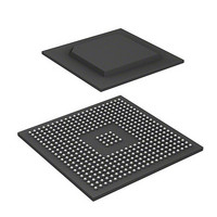
R8A77850BDBGV#RD0Z Renesas Electronics America, R8A77850BDBGV#RD0Z Datasheet - Page 782

R8A77850BDBGV#RD0Z
Manufacturer Part Number
R8A77850BDBGV#RD0Z
Description
IC SUPERH MPU ROMLESS 436BGA
Manufacturer
Renesas Electronics America
Series
SuperH® SH7780r
Datasheet
1.R8A77850AADBGV.pdf
(1694 pages)
Specifications of R8A77850BDBGV#RD0Z
Core Processor
SH-4A
Core Size
32-Bit
Speed
600MHz
Connectivity
Audio Codec, MMC, Serial Sound, SCI, SIO, SPI, SSI
Peripherals
DMA, POR, WDT
Number Of I /o
108
Program Memory Type
ROMless
Ram Size
8K x 8
Voltage - Supply (vcc/vdd)
1 V ~ 1.2 V
Oscillator Type
External
Operating Temperature
-40°C ~ 85°C
Package / Case
436-BGA
Lead Free Status / RoHS Status
Lead free / RoHS Compliant
Eeprom Size
-
Program Memory Size
-
Data Converters
-
Available stocks
Company
Part Number
Manufacturer
Quantity
Price
- Current page: 782 of 1694
- Download datasheet (9Mb)
15. Clock Pulse Generator (CPG)
4. Set H'CF000001 in FRQCR0 to enable execution of the sequence that changes the frequency.
5. The CLKOUTENB pin output changes to low level. After ten cycles of the peripheral clock
6. When the oscillation of PLL circuit 2 is stable, wait for ten cycles of the peripheral clock
7. When the WDT starts counting up and the value of WDTBCNT is equal to the value of
8. When H'00000000 is read from FRQCR0, the sequence that changes the frequency has
Note: * When setting a value except H'0 in the MFC3 to MFC0 bits in FRQCR1 to change the
Rev.1.00 Jan. 10, 2008 Page 750 of 1658
REJ09B0261-0100
PLL circuit 2 stabilized oscillation
CLKOUT
output
CLKOUTENB
output
The sequence that changes the frequency starts.
(Pck), an unstable clock is output to the CLKOUT pin.
(Pck). Then output a high level signal to the CLKOUTENB pin.
WDTBST, the LSI resumes operation.
finished. The internal clock has been changed to the clock with the specified division ratio.
CLKOUT
output
CLKOUTENB
output
DDR clock frequency, switch SDRAM to the self-refreshing state before executing
step (2) above. For details on how to switch to or release the self-refreshing state, see
section 12, DDR2-SDRAM Interface (DBSC2).
Figure 15.2 Beginning of the Change of the Bus Clock Frequency
Figure 15.3 End of the Change of the Bus Clock Frequency
Ten peripheral clock cycles
Ten peripheral clock cycles
Counting-up by the WDT
PLL circuit 2 oscillation starts
Operation restarts
Related parts for R8A77850BDBGV#RD0Z
Image
Part Number
Description
Manufacturer
Datasheet
Request
R

Part Number:
Description:
KIT STARTER FOR M16C/29
Manufacturer:
Renesas Electronics America
Datasheet:

Part Number:
Description:
KIT STARTER FOR R8C/2D
Manufacturer:
Renesas Electronics America
Datasheet:

Part Number:
Description:
R0K33062P STARTER KIT
Manufacturer:
Renesas Electronics America
Datasheet:

Part Number:
Description:
KIT STARTER FOR R8C/23 E8A
Manufacturer:
Renesas Electronics America
Datasheet:

Part Number:
Description:
KIT STARTER FOR R8C/25
Manufacturer:
Renesas Electronics America
Datasheet:

Part Number:
Description:
KIT STARTER H8S2456 SHARPE DSPLY
Manufacturer:
Renesas Electronics America
Datasheet:

Part Number:
Description:
KIT STARTER FOR R8C38C
Manufacturer:
Renesas Electronics America
Datasheet:

Part Number:
Description:
KIT STARTER FOR R8C35C
Manufacturer:
Renesas Electronics America
Datasheet:

Part Number:
Description:
KIT STARTER FOR R8CL3AC+LCD APPS
Manufacturer:
Renesas Electronics America
Datasheet:

Part Number:
Description:
KIT STARTER FOR RX610
Manufacturer:
Renesas Electronics America
Datasheet:

Part Number:
Description:
KIT STARTER FOR R32C/118
Manufacturer:
Renesas Electronics America
Datasheet:

Part Number:
Description:
KIT DEV RSK-R8C/26-29
Manufacturer:
Renesas Electronics America
Datasheet:

Part Number:
Description:
KIT STARTER FOR SH7124
Manufacturer:
Renesas Electronics America
Datasheet:

Part Number:
Description:
KIT STARTER FOR H8SX/1622
Manufacturer:
Renesas Electronics America
Datasheet:

Part Number:
Description:
KIT DEV FOR SH7203
Manufacturer:
Renesas Electronics America
Datasheet:


