MCIMX53-START Freescale Semiconductor, MCIMX53-START Datasheet - Page 104
MCIMX53-START
Manufacturer Part Number
MCIMX53-START
Description
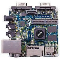
KIT DEVELOPMENT I.MX53
Manufacturer
Freescale Semiconductor
Series
i.MX53r
Type
MCUr
Datasheets
1.MCIMX53-START.pdf
(2 pages)
2.MCIMX53-START.pdf
(180 pages)
3.MCIMX53-START.pdf
(204 pages)
Specifications of MCIMX53-START
Contents
Board
Silicon Manufacturer
Freescale
Core Architecture
ARM
Core Sub-architecture
Cortex - A8
Silicon Core Number
I.MX5
Silicon Family Name
I.MX53
Peak Reflow Compatible (260 C)
Yes
Rohs Compliant
Yes
Leaded Process Compatible
Yes
Lead Free Status / RoHS Status
Lead free / RoHS Compliant
For Use With/related Products
i.MX53
Lead Free Status / Rohs Status
Supplier Unconfirmed
Available stocks
Company
Part Number
Manufacturer
Quantity
Price


Electrical Characteristics
4.7.8.9
The IPU supports the following types of asynchronous serial interfaces:
The IPU has four independent outputs and one input. The port can be configured to provide 3, 4, or 5-wire
interfaces.
Figure 56
active-low IPP#_CS signal and the straight polarity of the IPP_CLK signal.
For this interface, a bidirectional data line is used outside the chip. The IPU still uses separate input and
output data lines (IPP_IND_DISPB_SD_D and IPP_DO_DISPB_SD_D). The I/O mux should provide
joining the internal data lines to the bidirectional external line according to the IPP_OBE_DISPB_SD_D
signal provided by the IPU.
104
9
DISP_UP is predefined in REGISTER.
10
DISP_DOWN is predefined in REGISTER.
11
DISP_UP is predefined in REGISTER.
12
13
Note: DISP#_READ_EN—operand of DC’s MICROCDE READ command to sample incoming data.
14
chip-level output delay, board delays, a chip-level input delay, an IPU input delay. This value is chip specific.
Display control up for read
Display control down for read
Display control up for write
This parameter is a requirement to the display connected to the IPU.
Data read point
Loop back delay Tlbd is the cumulative propagation delay of read controls and read data. It includes an IPU output delay, a
1. 3-wire (with bidirectional data line).
2. 4-wire (with separate data input and output lines).
3. 5-wire type 1 (with sampling RS by the serial clock).
4. 5-wire type 2 (with sampling RS by the chip select signal).
depicts the timing diagram of the 3-wire serial interface. The timing diagrams correspond to
Standard Serial Interfaces
i.MX53xA Automotive and Infotainment Applications Processors, Rev. 1
Tdicdrw
Tdicuw
Tdicur
Tdrp
=
=
=
=
1
-- - T DI_CLK
2
1
-- - T DI_CLK
2
1
-- - T DI_CLK
2
T DI_CLK
⎛
⎝
⎛
⎝
⎛
⎝
×
×
×
ceil
×
ceil
ceil
ceil
DISP#_READ_EN
--------------------------------------------- -
DI_CLK_PERIOD
--------------------------------------------- -
DI_CLK_PERIOD
2
------------------------------------------------- -
--------------------------------------------- -
DI_CLK_PERIOD
DI_CLK_PERIOD
2
2
×
×
×
DISP_DOWN_#
DISP_UP_#
DISP_UP_#
⎞
⎠
⎞
⎠
⎞
⎠
Freescale Semiconductor
Related parts for MCIMX53-START
Image
Part Number
Description
Manufacturer
Datasheet
Request
R

Part Number:
Description:
MCIMX-LVDS1
Manufacturer:
Freescale Semiconductor
Datasheet:

Part Number:
Description:
Manufacturer:
Freescale Semiconductor, Inc
Datasheet:
Part Number:
Description:
Manufacturer:
Freescale Semiconductor, Inc
Datasheet:
Part Number:
Description:
Manufacturer:
Freescale Semiconductor, Inc
Datasheet:
Part Number:
Description:
Manufacturer:
Freescale Semiconductor, Inc
Datasheet:
Part Number:
Description:
Manufacturer:
Freescale Semiconductor, Inc
Datasheet:
Part Number:
Description:
Manufacturer:
Freescale Semiconductor, Inc
Datasheet:
Part Number:
Description:
Manufacturer:
Freescale Semiconductor, Inc
Datasheet:
Part Number:
Description:
Manufacturer:
Freescale Semiconductor, Inc
Datasheet:
Part Number:
Description:
Manufacturer:
Freescale Semiconductor, Inc
Datasheet:
Part Number:
Description:
Manufacturer:
Freescale Semiconductor, Inc
Datasheet:
Part Number:
Description:
Manufacturer:
Freescale Semiconductor, Inc
Datasheet:
Part Number:
Description:
Manufacturer:
Freescale Semiconductor, Inc
Datasheet:
Part Number:
Description:
Manufacturer:
Freescale Semiconductor, Inc
Datasheet:
Part Number:
Description:
Manufacturer:
Freescale Semiconductor, Inc
Datasheet: