MCIMX53-START Freescale Semiconductor, MCIMX53-START Datasheet - Page 115
MCIMX53-START
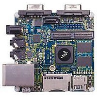
Manufacturer Part Number
MCIMX53-START
Description
KIT DEVELOPMENT I.MX53
Manufacturer
Freescale Semiconductor
Series
i.MX53r
Type
MCUr
Datasheets
1.MCIMX53-START.pdf
(2 pages)
2.MCIMX53-START.pdf
(180 pages)
3.MCIMX53-START.pdf
(204 pages)
Specifications of MCIMX53-START
Contents
Board
Silicon Manufacturer
Freescale
Core Architecture
ARM
Core Sub-architecture
Cortex - A8
Silicon Core Number
I.MX5
Silicon Family Name
I.MX53
Peak Reflow Compatible (260 C)
Yes
Rohs Compliant
Yes
Leaded Process Compatible
Yes
Lead Free Status / RoHS Status
Lead free / RoHS Compliant
For Use With/related Products
i.MX53
Lead Free Status / Rohs Status
Supplier Unconfirmed
Available stocks
Company
Part Number
Manufacturer
Quantity
Price


4.7.13
This section describes the timing parameters of the Parallel ATA module which are compliant with
ATA/ATAPI-6 specification.
Parallel ATA module can work on PIO/Multi-Word DMA/Ultra DMA transfer modes. Each transfer mode
has different data transfer rate, Ultra DMA mode 4 data transfer rate is up to 100MB/s. Parallel ATA
module interface consist of a total of 29 pins. Some pins act on different function in different transfer
mode. There are different requirements of timing relationships among the function pins conform with
ATA/ATAPI-6 specification and these requirements are configurable by the ATA module registers.
Table 69
modes.
Freescale Semiconductor
1
1
SRISE and SFALL shall meet this requirement when measured at the sender’s connector from 10–90% of full signal
amplitude with all capacitive loads from 15
CL of PWMO = 30 pF
SI1
SI2
SI3
Ref. No.
ID
2a
2b
3a
3b
4a
4b
1
ATA Interface Signals
Rising edge slew rate for any signal on ATA interface
Falling edge slew rate for any signal on ATA interface
Host interface signal capacitance at the host connector
and
PATA Timing Parameters
System CLK frequency
Clock high time
Clock low time
Clock fall time
Clock rise time
Output delay time
Output setup time
Figure 67
i.MX53xA Automotive and Infotainment Applications Processors, Rev. 1
define the AC characteristics of all the PATA interface signals in all data transfer
Table 69. AC Characteristics of All Interface Signals
Figure 67. PATA Interface Signals Timing Diagram
Parameter
Parameter
Table 68. PWM Output Timing Parameter
1
–
40 pF where all signals have the same capacitive load value.
SI2
1
1
12.29
9.91
8.71
Min
—
—
—
0
SI1
Symbol
C
S
S
host
rise
fall
Min
—
—
—
ipg_clk
Max
9.37
0.5
0.5
—
—
—
Electrical Characteristics
Max
1.25
1.25
20
MHz
Unit
ns
ns
ns
ns
ns
ns
Unit
V/ns
V/ns
pF
115
Related parts for MCIMX53-START
Image
Part Number
Description
Manufacturer
Datasheet
Request
R

Part Number:
Description:
MCIMX-LVDS1
Manufacturer:
Freescale Semiconductor
Datasheet:

Part Number:
Description:
Manufacturer:
Freescale Semiconductor, Inc
Datasheet:
Part Number:
Description:
Manufacturer:
Freescale Semiconductor, Inc
Datasheet:
Part Number:
Description:
Manufacturer:
Freescale Semiconductor, Inc
Datasheet:
Part Number:
Description:
Manufacturer:
Freescale Semiconductor, Inc
Datasheet:
Part Number:
Description:
Manufacturer:
Freescale Semiconductor, Inc
Datasheet:
Part Number:
Description:
Manufacturer:
Freescale Semiconductor, Inc
Datasheet:
Part Number:
Description:
Manufacturer:
Freescale Semiconductor, Inc
Datasheet:
Part Number:
Description:
Manufacturer:
Freescale Semiconductor, Inc
Datasheet:
Part Number:
Description:
Manufacturer:
Freescale Semiconductor, Inc
Datasheet:
Part Number:
Description:
Manufacturer:
Freescale Semiconductor, Inc
Datasheet:
Part Number:
Description:
Manufacturer:
Freescale Semiconductor, Inc
Datasheet:
Part Number:
Description:
Manufacturer:
Freescale Semiconductor, Inc
Datasheet:
Part Number:
Description:
Manufacturer:
Freescale Semiconductor, Inc
Datasheet:
Part Number:
Description:
Manufacturer:
Freescale Semiconductor, Inc
Datasheet: