MCIMX53-START Freescale Semiconductor, MCIMX53-START Datasheet - Page 27
MCIMX53-START
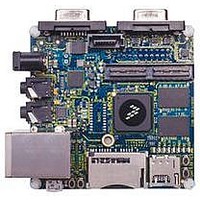
Manufacturer Part Number
MCIMX53-START
Description
KIT DEVELOPMENT I.MX53
Manufacturer
Freescale Semiconductor
Series
i.MX53r
Type
MCUr
Datasheets
1.MCIMX53-START.pdf
(2 pages)
2.MCIMX53-START.pdf
(180 pages)
3.MCIMX53-START.pdf
(204 pages)
Specifications of MCIMX53-START
Contents
Board
Silicon Manufacturer
Freescale
Core Architecture
ARM
Core Sub-architecture
Cortex - A8
Silicon Core Number
I.MX5
Silicon Family Name
I.MX53
Peak Reflow Compatible (260 C)
Yes
Rohs Compliant
Yes
Leaded Process Compatible
Yes
Lead Free Status / RoHS Status
Lead free / RoHS Compliant
For Use With/related Products
i.MX53
Lead Free Status / Rohs Status
Supplier Unconfirmed
Available stocks
Company
Part Number
Manufacturer
Quantity
Price


4.2.2
Power-down sequence should follow one of the following two options:
Option 1: Switch all supplies down simultaneously with further free discharge. A deviation of few
microseconds of actual power-down of the different power rails is acceptable.
Option 2: Switch down supplies, in any order, keeping the following rules:
4.2.3
4.3
This section includes the DC parameters of the following I/O types:
Freescale Semiconductor
•
•
•
•
•
•
•
•
•
•
•
•
Then the following rule should be kept: VDD_REG output impedance must be higher than 1 kΩ,
when inactive.
NVCC_CKIH must be powered down at the same time or after the UHVIO IO cell supplies. A
deviation of few microseconds of actual power-down of the different power rails is acceptable.
VDD_REG must be powered down at the same time or after NVCC_EMI_DRAM supply. A
deviation of few microseconds of actual power-down of the different power rails is acceptable.
If all of the following conditions are met:
— 1. VDD_REG is powered down to 0V (Not Hi-Z)
— 2. VDD_DIG_PLL and VDD_ANA_PLL are provided externally,
— 3. VDD_REG is powered down before VDD_DIG_PLL and VDD_ANA_PLL
All IO pins should not be externally driven while the IO power supply for the pin (NVCC_xxx) is
off. This can cause internal latch-up and malfunctions due to reverse current flows. For information
about IO power supply of each pin, see “Power Rail” columns in pin list tables of
“Package Information and Contact
If not using SATA interface and the embedded thermal sensor, the VP and VPH should be
grounded. In particular, keeping VPH turned OFF while the VP is powered ON is not
recommended and might lead to excessive power consumption.
When internal clock source is used for SATA temperature monitor the USB_PHY supplies and
PLL need to be active because they are providing the clock.
If not using TVE the module, the TVDAC_DHVDD and TVDAC_AHVDDRGB can remain
floating. If only the GPIO pads in TVDAC_AHVDDRGB domain are in use, the supplies can be
set to GPIO pad voltage range (1.65 V to 3.1 V).
General Purpose I/O (GPIO)
Double Data Rate 3 I/O (DDR3) for DDR2/LVDDR2, LPDDR2 and DDR3 modes
Low Voltage I/O (LVIO)
Ultra High Voltage I/O (UHVIO)
LVDS I/O
I/O DC Parameters
Power-Down Sequence
Power Supplies Usage
i.MX53xA Automotive and Infotainment Applications Processors, Rev. 1
Assignments.”
Electrical Characteristics
Section 6,
27
Related parts for MCIMX53-START
Image
Part Number
Description
Manufacturer
Datasheet
Request
R

Part Number:
Description:
MCIMX-LVDS1
Manufacturer:
Freescale Semiconductor
Datasheet:

Part Number:
Description:
Manufacturer:
Freescale Semiconductor, Inc
Datasheet:
Part Number:
Description:
Manufacturer:
Freescale Semiconductor, Inc
Datasheet:
Part Number:
Description:
Manufacturer:
Freescale Semiconductor, Inc
Datasheet:
Part Number:
Description:
Manufacturer:
Freescale Semiconductor, Inc
Datasheet:
Part Number:
Description:
Manufacturer:
Freescale Semiconductor, Inc
Datasheet:
Part Number:
Description:
Manufacturer:
Freescale Semiconductor, Inc
Datasheet:
Part Number:
Description:
Manufacturer:
Freescale Semiconductor, Inc
Datasheet:
Part Number:
Description:
Manufacturer:
Freescale Semiconductor, Inc
Datasheet:
Part Number:
Description:
Manufacturer:
Freescale Semiconductor, Inc
Datasheet:
Part Number:
Description:
Manufacturer:
Freescale Semiconductor, Inc
Datasheet:
Part Number:
Description:
Manufacturer:
Freescale Semiconductor, Inc
Datasheet:
Part Number:
Description:
Manufacturer:
Freescale Semiconductor, Inc
Datasheet:
Part Number:
Description:
Manufacturer:
Freescale Semiconductor, Inc
Datasheet:
Part Number:
Description:
Manufacturer:
Freescale Semiconductor, Inc
Datasheet: