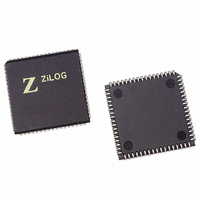
Z8S18033VSG Zilog, Z8S18033VSG Datasheet - Page 118

Z8S18033VSG
Manufacturer Part Number
Z8S18033VSG
Description
IC 33MHZ STATIC Z180 68-PLCC
Manufacturer
Zilog
Series
Z8018xr
Specifications of Z8S18033VSG
Processor Type
Z180
Features
Enhanced Z180
Speed
33MHz
Voltage
5V
Mounting Type
Surface Mount
Package / Case
68-LCC (J-Lead)
Core Size
8bit
Cpu Speed
33MHz
Digital Ic Case Style
PLCC
No. Of Pins
68
Supply Voltage Range
4.5V To 5.5V
Operating Temperature Range
0°C To +70°C
Svhc
No SVHC (18-Jun-2010)
Rohs Compliant
Yes
Processor Series
Z8S180X
Core
Z80
Data Bus Width
8 bit
Maximum Clock Frequency
33 MHz
Number Of Timers
2
Operating Supply Voltage
0 V to 3.3 V
Maximum Operating Temperature
+ 70 C
Mounting Style
SMD/SMT
Development Tools By Supplier
Z8S18000ZEM
Minimum Operating Temperature
0 C
Base Number
8
Lead Free Status / RoHS Status
Lead free / RoHS Compliant
Other names
269-4307
Q2431383
Z8S18033VSG
Q2431383
Z8S18033VSG
Available stocks
Company
Part Number
Manufacturer
Quantity
Price
Company:
Part Number:
Z8S18033VSG
Manufacturer:
Zilog
Quantity:
40
Company:
Part Number:
Z8S18033VSG
Manufacturer:
ZILOG
Quantity:
6 252
- Current page: 118 of 326
- Download datasheet (5Mb)
Bit
Position Bit/Field
2-0
DMA Register Description
Bit 7
This bit must be set to 1 only when both DMA channels are set to take
their requests from the same device. If this bit is 1 (it resets to 0), the
TEND output of DMA channel o sets a flip-flop, so that thereafter the
device’s request is visible to channel 1, but not visible to channel 0. The
internal TEND signal of channel 1 clears the FF, so that thereafter, the
device’s request is visible to channel 0, but no visible to channel 1.
If DMA request are from differing sources, DMA channel 0 request is
forced onto DMA channel 1 after TEND output of DMA channel 0 sets
the flop-flop to alternate.
Bit 6
When both DMA channels are programmed to take their requests from
the same device, this bit (FF mentioned in the previous paragraph)
controls which channel the device’s request is presented to: 0 = DMA0, 1
= DMA l. When Bit 7 is 1, this bit is automatically toggled by the channel
end output of the channels.
R/W
R/W
Value Description
000
001
010
011
111
DMA1 ext TOUT/DREQ
DMA1 ASCI0
DMA1 ASCI1
DMA1 ESCC
DMA1 PIA27-20 (P1284)
Family MPU User Manual
UM005003-0703
Z8018x
103
Related parts for Z8S18033VSG
Image
Part Number
Description
Manufacturer
Datasheet
Request
R

Part Number:
Description:
Z8S180 APPLICATION BOARD
Manufacturer:
Zilog
Datasheet:

Part Number:
Description:
Communication Controllers, ZILOG INTELLIGENT PERIPHERAL CONTROLLER (ZIP)
Manufacturer:
Zilog, Inc.
Datasheet:

Part Number:
Description:
KIT DEV FOR Z8 ENCORE 16K TO 64K
Manufacturer:
Zilog
Datasheet:

Part Number:
Description:
KIT DEV Z8 ENCORE XP 28-PIN
Manufacturer:
Zilog
Datasheet:

Part Number:
Description:
DEV KIT FOR Z8 ENCORE 8K/4K
Manufacturer:
Zilog
Datasheet:

Part Number:
Description:
KIT DEV Z8 ENCORE XP 28-PIN
Manufacturer:
Zilog
Datasheet:

Part Number:
Description:
DEV KIT FOR Z8 ENCORE 4K TO 8K
Manufacturer:
Zilog
Datasheet:

Part Number:
Description:
CMOS Z8 microcontroller. ROM 16 Kbytes, RAM 256 bytes, speed 16 MHz, 32 lines I/O, 3.0V to 5.5V
Manufacturer:
Zilog, Inc.
Datasheet:

Part Number:
Description:
Low-cost microcontroller. 512 bytes ROM, 61 bytes RAM, 8 MHz
Manufacturer:
Zilog, Inc.
Datasheet:

Part Number:
Description:
Z8 4K OTP Microcontroller
Manufacturer:
Zilog, Inc.
Datasheet:

Part Number:
Description:
CMOS SUPER8 ROMLESS MCU
Manufacturer:
Zilog, Inc.
Datasheet:

Part Number:
Description:
SL1866 CMOSZ8 OTP Microcontroller
Manufacturer:
Zilog, Inc.
Datasheet:

Part Number:
Description:
SL1866 CMOSZ8 OTP Microcontroller
Manufacturer:
Zilog, Inc.
Datasheet:

Part Number:
Description:
OTP (KB) = 1, RAM = 125, Speed = 12, I/O = 14, 8-bit Timers = 2, Comm Interfaces Other Features = Por, LV Protect, Voltage = 4.5-5.5V
Manufacturer:
Zilog, Inc.
Datasheet:


