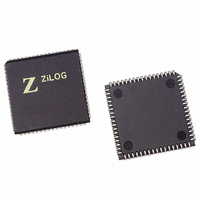
Z8S18033VSG Zilog, Z8S18033VSG Datasheet - Page 126

Z8S18033VSG
Manufacturer Part Number
Z8S18033VSG
Description
IC 33MHZ STATIC Z180 68-PLCC
Manufacturer
Zilog
Series
Z8018xr
Specifications of Z8S18033VSG
Processor Type
Z180
Features
Enhanced Z180
Speed
33MHz
Voltage
5V
Mounting Type
Surface Mount
Package / Case
68-LCC (J-Lead)
Core Size
8bit
Cpu Speed
33MHz
Digital Ic Case Style
PLCC
No. Of Pins
68
Supply Voltage Range
4.5V To 5.5V
Operating Temperature Range
0°C To +70°C
Svhc
No SVHC (18-Jun-2010)
Rohs Compliant
Yes
Processor Series
Z8S180X
Core
Z80
Data Bus Width
8 bit
Maximum Clock Frequency
33 MHz
Number Of Timers
2
Operating Supply Voltage
0 V to 3.3 V
Maximum Operating Temperature
+ 70 C
Mounting Style
SMD/SMT
Development Tools By Supplier
Z8S18000ZEM
Minimum Operating Temperature
0 C
Base Number
8
Lead Free Status / RoHS Status
Lead free / RoHS Compliant
Other names
269-4307
Q2431383
Z8S18033VSG
Q2431383
Z8S18033VSG
Available stocks
Company
Part Number
Manufacturer
Quantity
Price
Company:
Part Number:
Z8S18033VSG
Manufacturer:
Zilog
Quantity:
40
Company:
Part Number:
Z8S18033VSG
Manufacturer:
ZILOG
Quantity:
6 252
- Current page: 126 of 326
- Download datasheet (5Mb)
2. Specify memory « I/O transfer mode and address increment/
3. Load the number of bytes to transfer in BCR0
4. The DMA request sense mode (DMS0 bit in DCNTL) must be
5. Enable or disable DMA termination interrupt with the DIE0 bit in
6. Program DE0 =
The ASCI receiver or transmitter using DMA is initialized to allow the
first DMA transfer to begin.
The ASCI receiver must be empty as shown by RDRF =
The ASCI transmitter must be full as shown by TDRE = 0. Thus, the first
byte is written to the ASCI Transmit Data Register under program
control. The remaining bytes are transferred using DMA.
Channel 1 DMA
DMAC Channel 1 performs memory to/from I/O transfers. Except for
different registers and status/control bits, operation is exactly the same as
described for channel 0 memory to/from I/O DMA.
To initiate a DMA channel 1 memory to/from I/O transfer, perform the
following operations:
1. Load the memory address (20 bits) into MAR1.
2. Load the I/O address (16 bits) into IAR1.
3. Program the source/destination and address increment/decrement
decrement in the SM0, SM1, DM0 and DM1 bits of DMODE.
specified as edge sense.
DSTAT.
the DMA operation with the ASCI begins under control of the ASCI
generated internal DMA request.
mode using the DIM1 and DIM0 bits in DCNTL.
1
(with DWE0 =
0
in the same access) in DSTAT and
Family MPU User Manual
0
UM005003-0703
.
Z8018x
111
Related parts for Z8S18033VSG
Image
Part Number
Description
Manufacturer
Datasheet
Request
R

Part Number:
Description:
Z8S180 APPLICATION BOARD
Manufacturer:
Zilog
Datasheet:

Part Number:
Description:
Communication Controllers, ZILOG INTELLIGENT PERIPHERAL CONTROLLER (ZIP)
Manufacturer:
Zilog, Inc.
Datasheet:

Part Number:
Description:
KIT DEV FOR Z8 ENCORE 16K TO 64K
Manufacturer:
Zilog
Datasheet:

Part Number:
Description:
KIT DEV Z8 ENCORE XP 28-PIN
Manufacturer:
Zilog
Datasheet:

Part Number:
Description:
DEV KIT FOR Z8 ENCORE 8K/4K
Manufacturer:
Zilog
Datasheet:

Part Number:
Description:
KIT DEV Z8 ENCORE XP 28-PIN
Manufacturer:
Zilog
Datasheet:

Part Number:
Description:
DEV KIT FOR Z8 ENCORE 4K TO 8K
Manufacturer:
Zilog
Datasheet:

Part Number:
Description:
CMOS Z8 microcontroller. ROM 16 Kbytes, RAM 256 bytes, speed 16 MHz, 32 lines I/O, 3.0V to 5.5V
Manufacturer:
Zilog, Inc.
Datasheet:

Part Number:
Description:
Low-cost microcontroller. 512 bytes ROM, 61 bytes RAM, 8 MHz
Manufacturer:
Zilog, Inc.
Datasheet:

Part Number:
Description:
Z8 4K OTP Microcontroller
Manufacturer:
Zilog, Inc.
Datasheet:

Part Number:
Description:
CMOS SUPER8 ROMLESS MCU
Manufacturer:
Zilog, Inc.
Datasheet:

Part Number:
Description:
SL1866 CMOSZ8 OTP Microcontroller
Manufacturer:
Zilog, Inc.
Datasheet:

Part Number:
Description:
SL1866 CMOSZ8 OTP Microcontroller
Manufacturer:
Zilog, Inc.
Datasheet:

Part Number:
Description:
OTP (KB) = 1, RAM = 125, Speed = 12, I/O = 14, 8-bit Timers = 2, Comm Interfaces Other Features = Por, LV Protect, Voltage = 4.5-5.5V
Manufacturer:
Zilog, Inc.
Datasheet:


