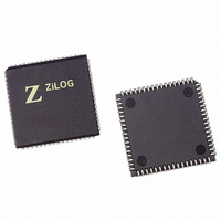
Z8S18033VSG Zilog, Z8S18033VSG Datasheet - Page 41

Z8S18033VSG
Manufacturer Part Number
Z8S18033VSG
Description
IC 33MHZ STATIC Z180 68-PLCC
Manufacturer
Zilog
Series
Z8018xr
Specifications of Z8S18033VSG
Processor Type
Z180
Features
Enhanced Z180
Speed
33MHz
Voltage
5V
Mounting Type
Surface Mount
Package / Case
68-LCC (J-Lead)
Core Size
8bit
Cpu Speed
33MHz
Digital Ic Case Style
PLCC
No. Of Pins
68
Supply Voltage Range
4.5V To 5.5V
Operating Temperature Range
0°C To +70°C
Svhc
No SVHC (18-Jun-2010)
Rohs Compliant
Yes
Processor Series
Z8S180X
Core
Z80
Data Bus Width
8 bit
Maximum Clock Frequency
33 MHz
Number Of Timers
2
Operating Supply Voltage
0 V to 3.3 V
Maximum Operating Temperature
+ 70 C
Mounting Style
SMD/SMT
Development Tools By Supplier
Z8S18000ZEM
Minimum Operating Temperature
0 C
Base Number
8
Lead Free Status / RoHS Status
Lead free / RoHS Compliant
Other names
269-4307
Q2431383
Z8S18033VSG
Q2431383
Z8S18033VSG
Available stocks
Company
Part Number
Manufacturer
Quantity
Price
Company:
Part Number:
Z8S18033VSG
Manufacturer:
Zilog
Quantity:
40
Company:
Part Number:
Z8S18033VSG
Manufacturer:
ZILOG
Quantity:
6 252
- Current page: 41 of 326
- Download datasheet (5Mb)
26
UM005003-0703
Z8018x
Family MPU User Manual
BUSREQ
BUSACK
RD, WR
A0
D0
MREQ
IORQ
When the bus is released, the address (A0–A19), data (D0–D7), and
control (MREQ, IORQ, RD, and WR) signals are placed in the high
impedance state.
Dynamic RAM refresh is not performed when the Z8X180 has released
the bus. The alternate bus master must provide dynamic memory
refreshing if the bus is released for long periods of time.
Figure 16 illustrates BUSREQ/BUSACK bus exchange during a memory
read cycle. Figure 17 illustrates bus exchange when the bus release is
requested during a Z8X180 CPU internal operation. BUSREQ is sampled
at the falling edge of the system clock prior to T3, T1 and Tx (BUS
RELEASE state). If BUSREQ is asserted Low at the falling edge of the
clock state prior to Tx, another Tx is executed.
Figure 16.
–
–
A19
Phi
D7
T1
Bus Exchange Timing During Memory Read
CPU memory read cycle
T2
TW
T3
TX
Bus release cycle
TX
T1
CPU cycle
T1
Related parts for Z8S18033VSG
Image
Part Number
Description
Manufacturer
Datasheet
Request
R

Part Number:
Description:
Z8S180 APPLICATION BOARD
Manufacturer:
Zilog
Datasheet:

Part Number:
Description:
Communication Controllers, ZILOG INTELLIGENT PERIPHERAL CONTROLLER (ZIP)
Manufacturer:
Zilog, Inc.
Datasheet:

Part Number:
Description:
KIT DEV FOR Z8 ENCORE 16K TO 64K
Manufacturer:
Zilog
Datasheet:

Part Number:
Description:
KIT DEV Z8 ENCORE XP 28-PIN
Manufacturer:
Zilog
Datasheet:

Part Number:
Description:
DEV KIT FOR Z8 ENCORE 8K/4K
Manufacturer:
Zilog
Datasheet:

Part Number:
Description:
KIT DEV Z8 ENCORE XP 28-PIN
Manufacturer:
Zilog
Datasheet:

Part Number:
Description:
DEV KIT FOR Z8 ENCORE 4K TO 8K
Manufacturer:
Zilog
Datasheet:

Part Number:
Description:
CMOS Z8 microcontroller. ROM 16 Kbytes, RAM 256 bytes, speed 16 MHz, 32 lines I/O, 3.0V to 5.5V
Manufacturer:
Zilog, Inc.
Datasheet:

Part Number:
Description:
Low-cost microcontroller. 512 bytes ROM, 61 bytes RAM, 8 MHz
Manufacturer:
Zilog, Inc.
Datasheet:

Part Number:
Description:
Z8 4K OTP Microcontroller
Manufacturer:
Zilog, Inc.
Datasheet:

Part Number:
Description:
CMOS SUPER8 ROMLESS MCU
Manufacturer:
Zilog, Inc.
Datasheet:

Part Number:
Description:
SL1866 CMOSZ8 OTP Microcontroller
Manufacturer:
Zilog, Inc.
Datasheet:

Part Number:
Description:
SL1866 CMOSZ8 OTP Microcontroller
Manufacturer:
Zilog, Inc.
Datasheet:

Part Number:
Description:
OTP (KB) = 1, RAM = 125, Speed = 12, I/O = 14, 8-bit Timers = 2, Comm Interfaces Other Features = Por, LV Protect, Voltage = 4.5-5.5V
Manufacturer:
Zilog, Inc.
Datasheet:


