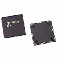
Z8S18033VSG Zilog, Z8S18033VSG Datasheet - Page 90

Z8S18033VSG
Manufacturer Part Number
Z8S18033VSG
Description
IC 33MHZ STATIC Z180 68-PLCC
Manufacturer
Zilog
Series
Z8018xr
Specifications of Z8S18033VSG
Processor Type
Z180
Features
Enhanced Z180
Speed
33MHz
Voltage
5V
Mounting Type
Surface Mount
Package / Case
68-LCC (J-Lead)
Core Size
8bit
Cpu Speed
33MHz
Digital Ic Case Style
PLCC
No. Of Pins
68
Supply Voltage Range
4.5V To 5.5V
Operating Temperature Range
0°C To +70°C
Svhc
No SVHC (18-Jun-2010)
Rohs Compliant
Yes
Processor Series
Z8S180X
Core
Z80
Data Bus Width
8 bit
Maximum Clock Frequency
33 MHz
Number Of Timers
2
Operating Supply Voltage
0 V to 3.3 V
Maximum Operating Temperature
+ 70 C
Mounting Style
SMD/SMT
Development Tools By Supplier
Z8S18000ZEM
Minimum Operating Temperature
0 C
Base Number
8
Lead Free Status / RoHS Status
Lead free / RoHS Compliant
Other names
269-4307
Q2431383
Z8S18033VSG
Q2431383
Z8S18033VSG
Available stocks
Company
Part Number
Manufacturer
Quantity
Price
Company:
Part Number:
Z8S18033VSG
Manufacturer:
Zilog
Quantity:
40
Company:
Part Number:
Z8S18033VSG
Manufacturer:
ZILOG
Quantity:
6 252
- Current page: 90 of 326
- Download datasheet (5Mb)
Figure 35.
INT0 - Maskable Interrupt Level 0
The next highest priority external interrupt after NMI is INT0. INT0 is
sampled at the falling edge of the clock state prior to T3 or T1 in the last
machine cycle. If INT0 is asserted LOW at the falling edge of the clock
state prior to T3 or T1 in the last machine cycle, INT0 is accepted. The
interrupt is masked if either the IEF1 flag or the ITEO (Interrupt Enable
0) bit in ITC are reset to
1. IEF1 is
2. ITE0 is
The INT0 interrupt is unique in that 3 programmable interrupt response
modes are available - Mode 0, Mode 1 and Mode 2. The specific mode is
selected with the IM 0, IM 1 and IM 2 (Set Interrupt Mode) instructions.
During RESET, the Z8X180 is initialized to use Mode 0 for INT0. The 3
interrupt response modes for INT0 are:
•
•
•
INT0 Mode 0
During the interrupt acknowledge cycle, an instruction is fetched from the
data bus (DO–D7) at the rising edge of T3. Often, this instruction is one
of the eight single byte RST (RESTART) instructions which stack the PC
and restart execution at a fixed logical address. However, multibyte
instructions can be processed if the interrupt acknowledging device can
provide a multibyte response. Unlike all other interrupts, the PC is not
automatically stacked:
Interrupts) instruction
Mode 0–Instruction fetch from data bus
Mode 1–Restart at logical address
Mode 2–Low-byte vector table address fetch from data bus
0
1
NMI Timing
, so INT0 is masked
, so INT0 is enabled by execution of the El (Enable
0
. After RESET the state is as follows:
0038H
Family MPU User Manual
UM005003-0703
Z8018x
75
Related parts for Z8S18033VSG
Image
Part Number
Description
Manufacturer
Datasheet
Request
R

Part Number:
Description:
Z8S180 APPLICATION BOARD
Manufacturer:
Zilog
Datasheet:

Part Number:
Description:
Communication Controllers, ZILOG INTELLIGENT PERIPHERAL CONTROLLER (ZIP)
Manufacturer:
Zilog, Inc.
Datasheet:

Part Number:
Description:
KIT DEV FOR Z8 ENCORE 16K TO 64K
Manufacturer:
Zilog
Datasheet:

Part Number:
Description:
KIT DEV Z8 ENCORE XP 28-PIN
Manufacturer:
Zilog
Datasheet:

Part Number:
Description:
DEV KIT FOR Z8 ENCORE 8K/4K
Manufacturer:
Zilog
Datasheet:

Part Number:
Description:
KIT DEV Z8 ENCORE XP 28-PIN
Manufacturer:
Zilog
Datasheet:

Part Number:
Description:
DEV KIT FOR Z8 ENCORE 4K TO 8K
Manufacturer:
Zilog
Datasheet:

Part Number:
Description:
CMOS Z8 microcontroller. ROM 16 Kbytes, RAM 256 bytes, speed 16 MHz, 32 lines I/O, 3.0V to 5.5V
Manufacturer:
Zilog, Inc.
Datasheet:

Part Number:
Description:
Low-cost microcontroller. 512 bytes ROM, 61 bytes RAM, 8 MHz
Manufacturer:
Zilog, Inc.
Datasheet:

Part Number:
Description:
Z8 4K OTP Microcontroller
Manufacturer:
Zilog, Inc.
Datasheet:

Part Number:
Description:
CMOS SUPER8 ROMLESS MCU
Manufacturer:
Zilog, Inc.
Datasheet:

Part Number:
Description:
SL1866 CMOSZ8 OTP Microcontroller
Manufacturer:
Zilog, Inc.
Datasheet:

Part Number:
Description:
SL1866 CMOSZ8 OTP Microcontroller
Manufacturer:
Zilog, Inc.
Datasheet:

Part Number:
Description:
OTP (KB) = 1, RAM = 125, Speed = 12, I/O = 14, 8-bit Timers = 2, Comm Interfaces Other Features = Por, LV Protect, Voltage = 4.5-5.5V
Manufacturer:
Zilog, Inc.
Datasheet:


