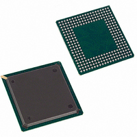
DS33R11+ Maxim Integrated Products, DS33R11+ Datasheet - Page 242

DS33R11+
Manufacturer Part Number
DS33R11+
Description
IC ETH TXRX T1/E1/J1 256-BGA
Manufacturer
Maxim Integrated Products
Type
Transceiverr
Datasheet
1.DS33R11.pdf
(344 pages)
Specifications of DS33R11+
Protocol
T1/E1/J1
Voltage - Supply
1.8V, 3.3V
Mounting Type
Surface Mount
Package / Case
256-BGA
Lead Free Status / RoHS Status
Lead free / RoHS Compliant
Number Of Drivers/receivers
-
- Current page: 242 of 344
- Download datasheet (12Mb)
Register Name:
Register Description:
Register Address:
Bit #
Name
Default
Bit 4: Line Interface Unit Mux Control (LIUC). This is a software version of the LIUC pin. When the LIUC pin is
connected high, the LIUC bit has control. When the LIUC pin is connected low, the framer and LIU are separated
and the LIUC bit has no effect.
Bit 3: Local Loopback (LLB). When this bit is set to 1, data continues to be transmitted as normal through the
transmit side of the transceiver. Data being received at RTIP and RRING are replaced with the data being
transmitted. Data in this loopback passes through the jitter attenuator. See
Bit 2: Remote Loopback (RLB). When this bit is set to 1, data input by the RPOSI and RNEGI pins is transmitted
back to the TPOSO and TNEGO pins. Data continues to pass through the receive-side framer of the transceiver as
it would normally. Data from the transmit-side formatter is ignored. See
Bit 1: Payload Loopback (PLB). When set to 1, payload loopback is enabled and the following occurs:
1) Data is transmitted from the TPOSO and TNEGO pins synchronous with RCLKO instead of TCLKT.
2) All the receive side signals continue to operate normally.
3) Data at the TSERI, TDATA, and TSIG pins is ignored.
T1 Mode: Normally, this loopback is only enabled when ESF framing is being performed but can also be enabled in
D4 framing applications. The transceiver loops the 192 bits of payload data (with BPVs corrected) from the receive
section back to the transmit section. The FPS framing pattern, CRC6 calculation, and the FDL bits are not looped
back; they are reinserted by the transceiver.
E1 Mode: The transceiver loops the 248 bits of payload data (with BPVs corrected) from the receive section back
to the transmit section. The transmit section modifies the payload as if it was input at TSERI. The FAS word; Si,
Sa, and E bits; and CRC4 are not looped back; they are reinserted by the transceiver.
Bit 0: Framer Loopback (FLB). When this bit is set to 1, the transceiver loops data from the transmit side back to
the receive side. When FLB is enabled, the following occurs:
1) T1 Mode: An unframed all-ones code is transmitted at TPOSO and TNEGO.
2) Data at RPOSI and RNEGI is ignored.
3) All receive-side signals take on timing synchronous with TCLKT instead of RDCLKI.
Please note that it is not acceptable to have RCLKO connected to TCLKT during this loopback because this
causes an unstable condition.
LIUC Pin
E1 Mode: Normal data is transmitted at TPOSO and TNEGO.
0
0
1
1
0 = LIU internally connected to framer.
1 = LIU disconnected from framer. Use TPOSI/TNEGI/TDCLKI/RPOSI/RNEGI/RDCLKI pins
—
7
0
LIUC Bit
0
1
0
1
TR.LBCR
Loopback Control Register
4Ah
—
6
0
LIU and framer separated
LIU and framer separated
LIU and framer connected
LIU and framer separated
Condition
—
5
0
242 of 344
LIUC
0
4
LLB
3
0
Figure 6-2
Figure 6-3
RLB
2
0
for more details.
for more details.
PLB
1
0
FLB
0
0
Related parts for DS33R11+
Image
Part Number
Description
Manufacturer
Datasheet
Request
R

Part Number:
Description:
MAX7528KCWPMaxim Integrated Products [CMOS Dual 8-Bit Buffered Multiplying DACs]
Manufacturer:
Maxim Integrated Products
Datasheet:

Part Number:
Description:
Single +5V, fully integrated, 1.25Gbps laser diode driver.
Manufacturer:
Maxim Integrated Products
Datasheet:

Part Number:
Description:
Single +5V, fully integrated, 155Mbps laser diode driver.
Manufacturer:
Maxim Integrated Products
Datasheet:

Part Number:
Description:
VRD11/VRD10, K8 Rev F 2/3/4-Phase PWM Controllers with Integrated Dual MOSFET Drivers
Manufacturer:
Maxim Integrated Products
Datasheet:

Part Number:
Description:
Highly Integrated Level 2 SMBus Battery Chargers
Manufacturer:
Maxim Integrated Products
Datasheet:

Part Number:
Description:
Current Monitor and Accumulator with Integrated Sense Resistor; ; Temperature Range: -40°C to +85°C
Manufacturer:
Maxim Integrated Products

Part Number:
Description:
TSSOP 14/A�/RS-485 Transceivers with Integrated 100O/120O Termination Resis
Manufacturer:
Maxim Integrated Products

Part Number:
Description:
TSSOP 14/A�/RS-485 Transceivers with Integrated 100O/120O Termination Resis
Manufacturer:
Maxim Integrated Products

Part Number:
Description:
QFN 16/A�/AC-DC and DC-DC Peak-Current-Mode Converters with Integrated Step
Manufacturer:
Maxim Integrated Products

Part Number:
Description:
TDFN/A/65V, 1A, 600KHZ, SYNCHRONOUS STEP-DOWN REGULATOR WITH INTEGRATED SWI
Manufacturer:
Maxim Integrated Products

Part Number:
Description:
Integrated Temperature Controller f
Manufacturer:
Maxim Integrated Products

Part Number:
Description:
SOT23-6/I�/45MHz to 650MHz, Integrated IF VCOs with Differential Output
Manufacturer:
Maxim Integrated Products

Part Number:
Description:
SOT23-6/I�/45MHz to 650MHz, Integrated IF VCOs with Differential Output
Manufacturer:
Maxim Integrated Products

Part Number:
Description:
EVALUATION KIT/2.4GHZ TO 2.5GHZ 802.11G/B RF TRANSCEIVER WITH INTEGRATED PA
Manufacturer:
Maxim Integrated Products

Part Number:
Description:
QFN/E/DUAL PCIE/SATA HIGH SPEED SWITCH WITH INTEGRATED BIAS RESISTOR
Manufacturer:
Maxim Integrated Products
Datasheet:


