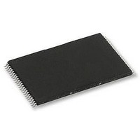
H27U8G8T2BTR-BC HYNIX SEMICONDUCTOR, H27U8G8T2BTR-BC Datasheet - Page 11

H27U8G8T2BTR-BC
Manufacturer Part Number
H27U8G8T2BTR-BC
Description
58T1893
Manufacturer
HYNIX SEMICONDUCTOR
Datasheet
1.H27U8G8T2BTR-BC.pdf
(52 pages)
Specifications of H27U8G8T2BTR-BC
Memory Type
Flash - NAND
Memory Size
8192Mbit
Memory Configuration
1024M X 8
Supply Voltage Range
2.7V To 3.6V
Memory Case Style
TSOP
No. Of Pins
48
Operating Temperature Range
0°C To +70°C
Rohs Compliant
Yes
Available stocks
Company
Part Number
Manufacturer
Quantity
Price
Company:
Part Number:
H27U8G8T2BTR-BC
Manufacturer:
HYNIX
Quantity:
10 000
Company:
Part Number:
H27U8G8T2BTR-BC
Manufacturer:
HYNIX
Quantity:
4 000
without an intervening erase operation, is allowed
in which up to 4,224 data bytes may be loaded into the data register, followed by a non-volatile memory programming
period where the loaded data are programmed into the appropriate cells.
input and then zero or more serial data input cycles. The words other than those to be programmed do not need to be
loaded. The device supports random data input in a page. The column address of next data, which will be entered, may
be changed to the address which follows random data input command (85h). Random data input may be operated multiple
times regardless of how many times it is done in a page.
tering the serial data will not initiate the programming process. The internal write state controller automatically executes
the algorithms and timings necessary for program and verify, thereby freeing the system controller for other tasks. Once
the program process starts, the Read Status Register command may be entered to read the status register. The system
controller can detect the completion of a program cycle by monitoring the R/B output, or the Status bit (I/O 6) of the Status
Register. Only the Read Status command and Reset command are accepted while programming is in progress. When the
Page Program is complete, the Write Status Bit (I/O 0) may be tested to check for fails in the program operation. The
internal write verify detects only errors for "1"s that are not successfully programmed to "0"s. The command register re-
mains in Read Status command mode until another valid command is written to the command register. Figure 15 and Fig-
ure 17 detail the sequence.
loaded into the data register, followed by a non-volatile memory programming period when the loaded data are pro-
grammed into the appropriate cells. The serial data loading period begins by inputting the Serial Data Input command
(80h), followed by the five address cycles input and then zero or more serial data for the 1st page. Address for this page
must be within 1st plane (A<20>=0) and A<19:13> and A<30:21> must be fixed low. Data of 1st page other than those
to be programmed do not need to be loaded. The device supports random data input exactly like a normal page program
operation. The Dummy Page Program Confirm command (11h) stops 1st page data input and the device goes busy for a
short time (tDBSY). Once it has returned ready, 81h command must be issued, followed by page address cycles and zero
or more serial data input cycles. Address for this page must be within 2nd plane (A<20>=1) and A<19:13> and A<30:21>
must be the valid addresses. The data of 2nd page other than those to be programmed do not need to be loaded. Program
Confirm command (10h) makes parallel programming of both pages start. User can check operation status by R/B pin or
read status register command, as if it were a normal page program; status register command is also available during Dum-
my Busy time (tDBSY).
each plane (IO0: total; IO1: plane0; IO2: plane1). Figure 16 details the sequence.
by an Erase Setup command (60h). Only addresses A20 to A30 are valid while A13 to A19 are ignored. The Erase Confirm
command (D0h) following the block address loading initiates the internal erasing process. This two-step sequence of setup
followed by execution command ensures that memory contents are not accidentally erased due to external noise condi-
tions.
verify.
controller can detect the completion of an erase by monitoring the RB# output, or the Status bit (I/O 6) of the Status
Register. Only the Read Status command and Reset command are valid while erasing is in progress. When the erase op-
eration is completed, the Write Status Bit (I/O 0) may be checked.
Rev 0.0 / Jul. 2008
3.3 Page Program
3.4 Multiplane Page Program
3.5 Block Erase
The device is programmed by page. Only a single partial or complete page programming operation within the same page,
The addressing must be done in sequential order in a block. A page program cycle consists of a serial data loading period
The serial data loading period begins by inputting the Serial Data Input command (80h), followed by five address cycles
The Page Program confirm command (10h) initiates the programming process. Writing 10h alone without previously en-
Device supports multiple plane program: it is possible to program in parallel 2 pages, one per each plane.
A multiple plane program cycle consists of a double serial data loading period in which up to 8,448 bytes of data may be
In case of fail in 1st or 2nd page program, fail bit of status register will be set: the device supports pass/fail status of
The Block Erase operation is done on a block basis. Block address loading is accomplished giving 3 address cycles initiated
At the rising edge of WE after the erase confirm command input, the internal write controller handles erase and erase-
Once the erase process starts, the Read Status Register command may be entered to read the status register. The system
Figure 18 details the sequence.
8 Gbit (1024 M x 8 bit) NAND Flash
H27U8G8T2B Series
Preliminary
11


