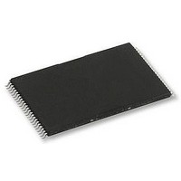
H27U8G8T2BTR-BC HYNIX SEMICONDUCTOR, H27U8G8T2BTR-BC Datasheet - Page 14

H27U8G8T2BTR-BC
Manufacturer Part Number
H27U8G8T2BTR-BC
Description
58T1893
Manufacturer
HYNIX SEMICONDUCTOR
Datasheet
1.H27U8G8T2BTR-BC.pdf
(52 pages)
Specifications of H27U8G8T2BTR-BC
Memory Type
Flash - NAND
Memory Size
8192Mbit
Memory Configuration
1024M X 8
Supply Voltage Range
2.7V To 3.6V
Memory Case Style
TSOP
No. Of Pins
48
Operating Temperature Range
0°C To +70°C
Rohs Compliant
Yes
Available stocks
Company
Part Number
Manufacturer
Quantity
Price
Company:
Part Number:
H27U8G8T2BTR-BC
Manufacturer:
HYNIX
Quantity:
10 000
Company:
Part Number:
H27U8G8T2BTR-BC
Manufacturer:
HYNIX
Quantity:
4 000
4. OTHER FEATURES
age detector disables all functions whenever Vcc is below about 2.0 V. WP pin provides hardware protection and is recom-
mended to be kept at V
for any command sequences as shown in Figure 28. The two-step command sequence for program/erase provides addi-
tional software protection.
back, cache program and random read completion. The R/B pin is normally high and goes to low when the device is busy
(after a reset, read, program, erase operation). It returns to high when the internal controller has finished the operation.
The pin is an open-drain driver thereby allowing two or more R/B outputs to be Or-tied. Because pull-up resistor value is
related to tr(R/B) and current drain during busy (I busy), an appropriate value can be obtained with the following reference
chart (Figure 29). Its value can be determined by the following guidance.
and 31. So, it is possible to connect NAND Flash to a microprocessor. The only function that was removed from standard
NAND Flash to make CE don't care operation was disabling of the automatic sequential read function.
Rev 0.0 / Jul. 2008
4.1 Data Protection
4.2 Ready/Busy
4.3 System Interface Using CE don't care
The device is designed to offer protection from any involuntary program/erase during power-transitions. An internal volt-
The device has a Ready/Busy output that provides method of indicating the completion of a page program, erase, copy-
To simplify system interface, CE may be deasserted during data loading or sequential data reading as shown Figure 30
IL
during power-up and power-down. A recovery time is required before internal circuit gets ready
8 Gbit (1024 M x 8 bit) NAND Flash
H27U8G8T2B Series
Preliminary
14


