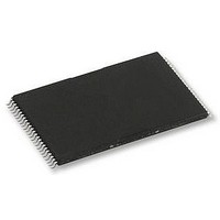
H27U8G8T2BTR-BC HYNIX SEMICONDUCTOR, H27U8G8T2BTR-BC Datasheet - Page 12

H27U8G8T2BTR-BC
Manufacturer Part Number
H27U8G8T2BTR-BC
Description
58T1893
Manufacturer
HYNIX SEMICONDUCTOR
Datasheet
1.H27U8G8T2BTR-BC.pdf
(52 pages)
Specifications of H27U8G8T2BTR-BC
Memory Type
Flash - NAND
Memory Size
8192Mbit
Memory Configuration
1024M X 8
Supply Voltage Range
2.7V To 3.6V
Memory Case Style
TSOP
No. Of Pins
48
Operating Temperature Range
0°C To +70°C
Rohs Compliant
Yes
Available stocks
Company
Part Number
Manufacturer
Quantity
Price
Company:
Part Number:
H27U8G8T2BTR-BC
Manufacturer:
HYNIX
Quantity:
10 000
Company:
Part Number:
H27U8G8T2BTR-BC
Manufacturer:
HYNIX
Quantity:
4 000
respectively (3 cycles each). As for block erase, D0h command makes this operation start.
can be checked like for multiple plane program. Figure 19 details the sequence.
out data reloading when the bit error is not in data stored. Since the time-consuming re-loading cycles are removed, the
system performance is improved. The benefit is especially obvious when a portion of block is updated and the rest of the
block also needs to be copied to the newly assigned free block. Copy-Back operation is a sequential execution of Read for
Copy-Back and of copy-back program with the destination page address. A read operation with "35h" command and the
address of the source page moves the whole 4,224-byte into the internal data buffer. A bit error is checked by reading
sequentially the data output. In the case where there is no bit error, the data do not need to be reloaded. Therefore Copy-
Back program operation is initiated by issuing Page-Copy Data-Input command (85h) with destination page address. Actual
programming operation begins after Program Confirm command (10h) is issued. Once the program process starts, the
Read Status Register command (70h) may be entered to read the status register. The system controller can detect the
completion of a program cycle by monitoring the RB# output, or the Status bit (I/O 6) of the Status Register.
ister remains in Read Status command mode until another valid command is written to the command register. During copy-
back program, data modification is possible using random data input command (85h) as shown in Figure 21.
As for single plane copy-back, a multi plane read operation with "35h" (multi plane read for copy-back) command and the
address of the source pages moves the whole 4,224-byte of each page into the internal data buffer of each plane. Since
the device is equipped with two memory planes, activating the two sets of 4,224 byte page registers enables a simultane-
ous programming of two pages. Figure 22 and Figure 23 show the details of the command sequence for the multi-plane
copy-back operation in standard operation mode. In order to reduce the buffer size required by host side (8KB buffer size)
to perform this operation, new Multiplane Copy-Back Program flows have been introduced as shown from Figure 24 to
Figure 25. As depictured the sequences of data out followed by data input for each plane can be performed an indefinite
number of times, which depend on the buffer size used by host (e.g. Figure 24 shows the sequence for a host equipped
with a 4KB buffer size, whereas the Figure 25 shows the sequence for a host equipped with 2KB buffer size).
pleted, and whether the program or erase operation is completed successfully. After writing 70h command to the command
register, a read cycle outputs the content of the Status Register to the I/O pins on the falling edge of CE or RE, whichever
occurs last. This two line control allows the system to poll the progress of each device in multiple memory connections
even when R/B pins are common-wired. RE or CE does not need to be toggled for updated status. Refer to Table 13 for
specific Status Register definitions and to Figure 10 for Status Read sequence. The command register remains in Status
Read mode until further commands are issued to it. Therefore, if the status register is read during a random read cycle,
the read command (00h) should be given before starting new read cycles.
Rev 0.0 / Jul. 2008
3.6 Multiplane Block Erase
3.7 Copy Back Program
3.8 Multiplane Copy Back Program
3.9 Read Status Register
Multiple plane erase allows parallel erase of two blocks, one per each plane.
Block erase setup command (60h) must be repeated two times, each time followed by 1st and 2nd block address cycles
Multi-plane erase does not need any Dummy Busy Time between 1st and 2nd block address cycles insertion.
Address limitation required for multiple plane program applies also to multiple plane erase, as well as operation progress
Copy-Back program with Read for Copy-Back is configured to quickly and efficiently rewrite data stored in one page with-
When the Copy-Back Program is complete, the Write Status Bit (I/O 0) may be checked (Figure 20). The command reg-
Copy-Back Program operation is allowed only within the same memory plane.
Two-Plane Copy-Back Program is an extension of Copy-Back Program, for a single plane with 4,224 byte page registers.
The device contains a Status Register which may be read to find out whether a read, program or erase operation is com-
8 Gbit (1024 M x 8 bit) NAND Flash
H27U8G8T2B Series
Preliminary
12


