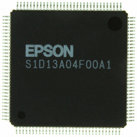
S1D13A04F00A Epson Electronics America Inc-Semiconductor Div, S1D13A04F00A Datasheet - Page 30

S1D13A04F00A
Manufacturer Part Number
S1D13A04F00A
Description
IC LCD COMPANION 160KB 128-TQFP
Manufacturer
Epson Electronics America Inc-Semiconductor Div
Specifications of S1D13A04F00A
Display Type
LCD
Voltage - Supply
1.8 V ~ 2.75 V
Mounting Type
Surface Mount
Package / Case
125-TQFP, 125-VQFP
Lead Free Status / RoHS Status
Lead free / RoHS Compliant
Current - Supply
-
Operating Temperature
-
Interface
-
Configuration
-
Digits Or Characters
-
Other names
S1D13A04F00A100
S1D13A04F00A100
S1D13A04F00A100
Available stocks
Company
Part Number
Manufacturer
Quantity
Price
Company:
Part Number:
S1D13A04F00A
Manufacturer:
Epson Electronics America Inc-Semiconductor Div
Quantity:
10 000
Company:
Part Number:
S1D13A04F00A1
Manufacturer:
EPSON
Quantity:
816
Part Number:
S1D13A04F00A1
Manufacturer:
EPSON/爱普生
Quantity:
20 000
Company:
Part Number:
S1D13A04F00A100
Manufacturer:
OSRAM
Quantity:
4 600
- Current page: 30 of 598
- Download datasheet (6Mb)
Page 24
S1D13A04
X37A-A-001-06
Pin Name
RD/WR#
M/R#
BS#
RD#
Type
I
I
I
I
PFBGA
Pin #
E3
E2
F3
E1
TQFP15
Pin#
10
11
15
12
Table 4-2: Host Interface Pin Descriptions
Cell
LI
LI
LI
LI
RESET#
State
—
—
—
—
Revision 6.0
This input pin is used to select between the display buffer and
register address spaces of the S1D13A04. M/R# is set high to
access the display buffer and low to access the registers. See
Table 4-8: “Host Bus Interface Pin Mapping,” on page 31 for
summary.
This input pin has multiple functions.
See Table 4-8: “Host Bus Interface Pin Mapping,” on page 31
for summary.
This input pin has multiple functions.
See Table 4-8: “Host Bus Interface Pin Mapping,” on page 31
for summary.
This input pin has multiple functions.
See Table 4-8: “Host Bus Interface Pin Mapping,” on page 31
for summary.
• For Generic #1, this pin must be tied to IO V
• For Generic #2, this pin must be tied to IO V
• For SH-3/SH-4, this pin inputs the bus start signal (BS#).
• For MC68K #1, this pin inputs the address strobe (AS#).
• For MC68K #2, this pin inputs the address strobe (AS#).
• For REDCAP2, this pin must be tied to IO V
• For DragonBall, this pin must be tied to IO V
• For Generic #1, this pin inputs the read command for the
• For Generic #2, this pin must be tied to IO V
• For SH-3/SH-4, this pin inputs the RD/WR# signal. The
• For MC68K #1, this pin inputs the R/W# signal.
• For MC68K #2, this pin inputs the R/W# signal.
• For REDCAP2, this pin inputs the R/W signal.
• For DragonBall, this pin must be tied to IO V
• For Generic #1, this pin inputs the read command for the
• For Generic #2, this pin inputs the read command (RD#).
• For SH-3/SH-4, this pin inputs the read signal (RD#).
• For MC68K #1, this pin must be tied to IO V
• For MC68K #2, this pin inputs the bus size bit 1 (SIZ1).
• For REDCAP2, this pin inputs the output enable (OE).
• For DragonBall, this pin inputs the output enable (OE).
upper data byte (RD1#).
S1D13A04 needs this signal for early decode of the bus
cycle.
lower data byte (RD0#).
Description
Epson Research and Development
Hardware Functional Specification
Vancouver Design Center
Issue Date: 2003/05/01
DD
DD
DD
DD
DD
DD
DD
.
.
.
.
.
.
.
Related parts for S1D13A04F00A
Image
Part Number
Description
Manufacturer
Datasheet
Request
R

Part Number:
Description:
IC CONTROLLER CRT/LCD/TV 128-QFP
Manufacturer:
Epson Electronics America Inc-Semiconductor Div
Part Number:
Description:
IC GRAPHIC LCD CTRLR 256-PBGA
Manufacturer:
Epson Electronics America Inc-Semiconductor Div
Datasheet:
Part Number:
Description:
MEMORY CARD 2M STATIC RAM
Manufacturer:
Epson Electronics America Inc-Semiconductor Div
Part Number:
Description:
IC CTRLR/PHY USB OTG 64-QFP
Manufacturer:
Epson Electronics America Inc-Semiconductor Div
Part Number:
Description:
IC CONTROLLER USB 2.0 64-QFP
Manufacturer:
Epson Electronics America Inc-Semiconductor Div

Part Number:
Description:
IC PHY CONT 2PORT 1394A 100-QFP
Manufacturer:
Epson Electronics America Inc-Semiconductor Div
Part Number:
Description:
IC LINK CTRLR 1394 IDE-33 184QFP
Manufacturer:
Epson Electronics America Inc-Semiconductor Div
Part Number:
Description:
IC LINK CTRLR 1394 IDE-66 184QFP
Manufacturer:
Epson Electronics America Inc-Semiconductor Div

Part Number:
Description:
IC LINK CTRLR 1394 IDE100 100QFP
Manufacturer:
Epson Electronics America Inc-Semiconductor Div

Part Number:
Description:
IC LINK CTRLR/PHY 1394 100-QFP
Manufacturer:
Epson Electronics America Inc-Semiconductor Div
Part Number:
Description:
IC CTRLR/PHY USB 2.0 64-QFP
Manufacturer:
Epson Electronics America Inc-Semiconductor Div

Part Number:
Description:
IC CTRLR/PHY USB 2.0 100-QFP
Manufacturer:
Epson Electronics America Inc-Semiconductor Div
Part Number:
Description:
IC CHARGE CTRLR LI-ION 24-SSOP
Manufacturer:
Epson Electronics America Inc-Semiconductor Div
Part Number:
Description:
IC BATTERY LEAK PREVENTION SOT89
Manufacturer:
Epson Electronics America Inc-Semiconductor Div
Part Number:
Description:
IC BATTERY LEAK PREVENTION SOT89
Manufacturer:
Epson Electronics America Inc-Semiconductor Div


