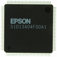
S1D13A04F00A Epson Electronics America Inc-Semiconductor Div, S1D13A04F00A Datasheet - Page 450

S1D13A04F00A
Manufacturer Part Number
S1D13A04F00A
Description
IC LCD COMPANION 160KB 128-TQFP
Manufacturer
Epson Electronics America Inc-Semiconductor Div
Specifications of S1D13A04F00A
Display Type
LCD
Voltage - Supply
1.8 V ~ 2.75 V
Mounting Type
Surface Mount
Package / Case
125-TQFP, 125-VQFP
Lead Free Status / RoHS Status
Lead free / RoHS Compliant
Current - Supply
-
Operating Temperature
-
Interface
-
Configuration
-
Digits Or Characters
-
Other names
S1D13A04F00A100
S1D13A04F00A100
S1D13A04F00A100
Available stocks
Company
Part Number
Manufacturer
Quantity
Price
Company:
Part Number:
S1D13A04F00A
Manufacturer:
Epson Electronics America Inc-Semiconductor Div
Quantity:
10 000
Company:
Part Number:
S1D13A04F00A1
Manufacturer:
EPSON
Quantity:
816
Part Number:
S1D13A04F00A1
Manufacturer:
EPSON/爱普生
Quantity:
20 000
Company:
Part Number:
S1D13A04F00A100
Manufacturer:
OSRAM
Quantity:
4 600
- Current page: 450 of 598
- Download datasheet (6Mb)
Page 8
2 Interfacing to the PC Card Bus
2.1 The PC Card System Bus
2.1.1 PC Card Overview
2.1.2 Memory Access Cycles
S1D13A04
X37A-G-005-01
Note
PC Card technology has gained wide acceptance in the mobile computing field as well as
in other markets due to its portability and ruggedness. This section is an overview of the
operation of the 16-bit PC Card interface conforming to the PCMCIA 2.0/JEIDA 4.1
Standard (or later).
The 16-bit PC Card provides a 26-bit address bus and additional control lines which allow
access to three 64M byte address ranges. These ranges are used for common memory space,
IO space, and attribute memory space. Common memory may be accessed by a host system
for memory read and write operations. Attribute memory is used for defining card specific
information such as configuration registers, card capabilities, and card use. IO space
maintains software and hardware compatibility with hosts such as the Intel x86 archi-
tecture, which address peripherals independently from memory space.
Bit notation follows the convention used by most microprocessors, the high bit is the most
significant. Therefore, signals A25 and D15 are the most significant bits for the address and
data bus respectively.
Support is provided for on-chip DMA controllers. To find further information on these
topics, refer to Section 6, “References” on page 15.
PC Card bus signals are asynchronous to the host CPU bus signals. Bus cycles are started
with the assertion of either the -CE1 and/or the -CE2 card enable signals. The cycle ends
once these signals are de-asserted. Bus cycles can be lengthened using the -WAIT signal.
A data transfer is initiated when the memory address is placed on the PC Card bus and one,
or both, of the card enable signals (-CE1 and -CE2) are driven low. -REG must be kept
inactive. If only -CE1 is driven low, 8-bit data transfers are enabled and A0 specifies
whether the even or odd data byte appears on data bus lines D[7:0]. If both -CE1 and -CE2
are driven low, a 16-bit word transfer takes place. If only -CE2 is driven low, an odd byte
transfer occurs on data lines D[15:8].
The PCMCIA 2.0/JEIDA 4.1 (and later) PC Card Standard support the two signals
-WAIT and RESET which are not supported in earlier versions of the standard. The
-WAIT signal allows for asynchronous data transfers for memory, attribute, and IO ac-
cess cycles. The RESET signal allows resetting of the card configuration by the reset
line of the host CPU.
Epson Research and Development
Interfacing to the PC Card Bus
Vancouver Design Center
Issue Date: 01/10/12
Related parts for S1D13A04F00A
Image
Part Number
Description
Manufacturer
Datasheet
Request
R

Part Number:
Description:
IC CONTROLLER CRT/LCD/TV 128-QFP
Manufacturer:
Epson Electronics America Inc-Semiconductor Div
Part Number:
Description:
IC GRAPHIC LCD CTRLR 256-PBGA
Manufacturer:
Epson Electronics America Inc-Semiconductor Div
Datasheet:
Part Number:
Description:
MEMORY CARD 2M STATIC RAM
Manufacturer:
Epson Electronics America Inc-Semiconductor Div
Part Number:
Description:
IC CTRLR/PHY USB OTG 64-QFP
Manufacturer:
Epson Electronics America Inc-Semiconductor Div
Part Number:
Description:
IC CONTROLLER USB 2.0 64-QFP
Manufacturer:
Epson Electronics America Inc-Semiconductor Div

Part Number:
Description:
IC PHY CONT 2PORT 1394A 100-QFP
Manufacturer:
Epson Electronics America Inc-Semiconductor Div
Part Number:
Description:
IC LINK CTRLR 1394 IDE-33 184QFP
Manufacturer:
Epson Electronics America Inc-Semiconductor Div
Part Number:
Description:
IC LINK CTRLR 1394 IDE-66 184QFP
Manufacturer:
Epson Electronics America Inc-Semiconductor Div

Part Number:
Description:
IC LINK CTRLR 1394 IDE100 100QFP
Manufacturer:
Epson Electronics America Inc-Semiconductor Div

Part Number:
Description:
IC LINK CTRLR/PHY 1394 100-QFP
Manufacturer:
Epson Electronics America Inc-Semiconductor Div
Part Number:
Description:
IC CTRLR/PHY USB 2.0 64-QFP
Manufacturer:
Epson Electronics America Inc-Semiconductor Div

Part Number:
Description:
IC CTRLR/PHY USB 2.0 100-QFP
Manufacturer:
Epson Electronics America Inc-Semiconductor Div
Part Number:
Description:
IC CHARGE CTRLR LI-ION 24-SSOP
Manufacturer:
Epson Electronics America Inc-Semiconductor Div
Part Number:
Description:
IC BATTERY LEAK PREVENTION SOT89
Manufacturer:
Epson Electronics America Inc-Semiconductor Div
Part Number:
Description:
IC BATTERY LEAK PREVENTION SOT89
Manufacturer:
Epson Electronics America Inc-Semiconductor Div


