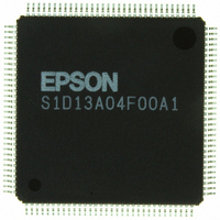
S1D13A04F00A Epson Electronics America Inc-Semiconductor Div, S1D13A04F00A Datasheet - Page 453

S1D13A04F00A
Manufacturer Part Number
S1D13A04F00A
Description
IC LCD COMPANION 160KB 128-TQFP
Manufacturer
Epson Electronics America Inc-Semiconductor Div
Specifications of S1D13A04F00A
Display Type
LCD
Voltage - Supply
1.8 V ~ 2.75 V
Mounting Type
Surface Mount
Package / Case
125-TQFP, 125-VQFP
Lead Free Status / RoHS Status
Lead free / RoHS Compliant
Current - Supply
-
Operating Temperature
-
Interface
-
Configuration
-
Digits Or Characters
-
Other names
S1D13A04F00A100
S1D13A04F00A100
S1D13A04F00A100
Available stocks
Company
Part Number
Manufacturer
Quantity
Price
Company:
Part Number:
S1D13A04F00A
Manufacturer:
Epson Electronics America Inc-Semiconductor Div
Quantity:
10 000
Company:
Part Number:
S1D13A04F00A1
Manufacturer:
EPSON
Quantity:
816
Part Number:
S1D13A04F00A1
Manufacturer:
EPSON/爱普生
Quantity:
20 000
Company:
Part Number:
S1D13A04F00A100
Manufacturer:
OSRAM
Quantity:
4 600
- Current page: 453 of 598
- Download datasheet (6Mb)
Epson Research and Development
Vancouver Design Center
3.2 Host Bus Interface Signals
Interfacing to the PC Card Bus
Issue Date: 01/10/12
The S1D13A04 Generic #2 Host Bus Interface requires the following signals from the PC
Card bus.
• CLKI is a clock input which is required by the S1D13A04 Host Bus Interface as a
• The address inputs AB[17:0], and the data bus DB[15:0], connect directly to the PC
• Chip Select (CS#) is driven by decoding the high-order address lines to select the proper
• M/R# (memory/register) selects between memory or register accesses. This signal is
• WE1# connects to -CE2 (the high byte chip select signal from the PC Card interface)
• WE0# connects to -WE (the write enable signal form the PC Card bus) and must be
• RD# connects to -OE (the read enable signal from the PC Card bus) and must be driven
• WAIT# is a signal output from the S1D13A04 that indicates the PC Card bus must wait
• The Bus Status (BS#) and Read/Write (RD/WR#) signals are not used in this implemen-
• The RESET# (active low) input of the S1D13A04 may be connected to the PC Card
source for its internal bus and memory clocks. This clock is typically driven by the host
CPU system clock. Since the PC Card signalling is independent of any clock, CLKI can
come from any oscillator already implemented. For example, the source for the CLKI2
input of the S1D13A04 may be used.
Card address (A[17:0]) and data bus (D[15:0]), respectively. CNF4 must be set to select
little endian mode.
register and memory address space.
generated by the external address decode circuitry. For this example, M/R# is connected
to address line A18, allowing system address A18 to select between memory or register
accesses.
which in conjunction with address bit 0 allows byte steering of read and write opera-
tions.
driven low when the PC Card bus is writing data to the S1D13A04.
low when the PC Card bus is reading data from the S1D13A04.
until data is ready (read cycle) or accepted (write cycle) on the host bus. Since PC Card
bus accesses to the S1D13A04 may occur asynchronously to the display update, it is
possible that contention may occur in accessing the S1D13A04 internal registers and/or
display buffer. The WAIT# line resolves these contentions by forcing the host to wait
until the resource arbitration is complete.
tation of the PC Card bus using the Generic #2 Host Bus Interface. These pins must be
tied high (connected to IO V
RESET (active high) using an inverter.
DD
).
X37A-G-005-01
S1D13A04
Page 11
Related parts for S1D13A04F00A
Image
Part Number
Description
Manufacturer
Datasheet
Request
R

Part Number:
Description:
IC CONTROLLER CRT/LCD/TV 128-QFP
Manufacturer:
Epson Electronics America Inc-Semiconductor Div
Part Number:
Description:
IC GRAPHIC LCD CTRLR 256-PBGA
Manufacturer:
Epson Electronics America Inc-Semiconductor Div
Datasheet:
Part Number:
Description:
MEMORY CARD 2M STATIC RAM
Manufacturer:
Epson Electronics America Inc-Semiconductor Div
Part Number:
Description:
IC CTRLR/PHY USB OTG 64-QFP
Manufacturer:
Epson Electronics America Inc-Semiconductor Div
Part Number:
Description:
IC CONTROLLER USB 2.0 64-QFP
Manufacturer:
Epson Electronics America Inc-Semiconductor Div

Part Number:
Description:
IC PHY CONT 2PORT 1394A 100-QFP
Manufacturer:
Epson Electronics America Inc-Semiconductor Div
Part Number:
Description:
IC LINK CTRLR 1394 IDE-33 184QFP
Manufacturer:
Epson Electronics America Inc-Semiconductor Div
Part Number:
Description:
IC LINK CTRLR 1394 IDE-66 184QFP
Manufacturer:
Epson Electronics America Inc-Semiconductor Div

Part Number:
Description:
IC LINK CTRLR 1394 IDE100 100QFP
Manufacturer:
Epson Electronics America Inc-Semiconductor Div

Part Number:
Description:
IC LINK CTRLR/PHY 1394 100-QFP
Manufacturer:
Epson Electronics America Inc-Semiconductor Div
Part Number:
Description:
IC CTRLR/PHY USB 2.0 64-QFP
Manufacturer:
Epson Electronics America Inc-Semiconductor Div

Part Number:
Description:
IC CTRLR/PHY USB 2.0 100-QFP
Manufacturer:
Epson Electronics America Inc-Semiconductor Div
Part Number:
Description:
IC CHARGE CTRLR LI-ION 24-SSOP
Manufacturer:
Epson Electronics America Inc-Semiconductor Div
Part Number:
Description:
IC BATTERY LEAK PREVENTION SOT89
Manufacturer:
Epson Electronics America Inc-Semiconductor Div
Part Number:
Description:
IC BATTERY LEAK PREVENTION SOT89
Manufacturer:
Epson Electronics America Inc-Semiconductor Div


