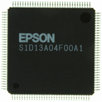
S1D13A04F00A Epson Electronics America Inc-Semiconductor Div, S1D13A04F00A Datasheet - Page 55

S1D13A04F00A
Manufacturer Part Number
S1D13A04F00A
Description
IC LCD COMPANION 160KB 128-TQFP
Manufacturer
Epson Electronics America Inc-Semiconductor Div
Specifications of S1D13A04F00A
Display Type
LCD
Voltage - Supply
1.8 V ~ 2.75 V
Mounting Type
Surface Mount
Package / Case
125-TQFP, 125-VQFP
Lead Free Status / RoHS Status
Lead free / RoHS Compliant
Current - Supply
-
Operating Temperature
-
Interface
-
Configuration
-
Digits Or Characters
-
Other names
S1D13A04F00A100
S1D13A04F00A100
S1D13A04F00A100
Available stocks
Company
Part Number
Manufacturer
Quantity
Price
Company:
Part Number:
S1D13A04F00A
Manufacturer:
Epson Electronics America Inc-Semiconductor Div
Quantity:
10 000
Company:
Part Number:
S1D13A04F00A1
Manufacturer:
EPSON
Quantity:
816
Part Number:
S1D13A04F00A1
Manufacturer:
EPSON/爱普生
Quantity:
20 000
Company:
Part Number:
S1D13A04F00A100
Manufacturer:
OSRAM
Quantity:
4 600
- Current page: 55 of 598
- Download datasheet (6Mb)
Epson Research and Development
Vancouver Design Center
1. The cycle length for the REDCAP interface is fixed.
2. The Read and Write 2D BitBLT functions are not available when using the REDCAP interface.
Hardware Functional Specification
Issue Date: 2003/05/01
Symbol
T
f
CKO
t6a
t6b
t6d
t10
t11
t12
t6c
CKO
t1
t2
t3
t4
t5
t7
t8
t9
Bus clock frequency
Bus clock period
A[16:1], R/W, CSn# setup to CKO rising edge
EB0,EB1 setup to CKO rising edge (write)
D[15:0] input setup to 4th CKO rising edge after CSn# and EB0 or
EB1 asserted low (write cycle)
D[15:0] input hold from 4th CKO rising edge after CSn# and EB0 or
EB1 asserted low (write cycle)
EB0,EB1,OE setup to CKO rising edge (read cycle)
1st CKO rising edge after CSn#, EB0 or EB1,OE asserted low to
D[15:0] valid for MCLK = BCLK (read cycle)
1st CKO rising edge after CSn#, EB0 or EB1,OE asserted low to
D[15:0] valid for MCLK = BCLK
1st CKO rising edge after CSn#, EB0 or EB1,OE asserted low to
D[15:0] valid for MCLK = BCLK
1st CKO rising edge after CSn#, EB0 or EB1,OE asserted low to
D[15:0] valid for MCLK = BCLK
EB0,EB1,OE falling edge to D[15:0] driven (read cycle)
A[16:1], R/W, CSn hold from CKO rising edge
EB0, EB1 setup to CKO rising edge (write cycle)
CKO falling edge to EB0, EB1, OE deasserted (read)
OE, EB0, EB1 deasserted to D[15:0] output high impedance (read)
Cycle Length (note 1)
Table 6-14: Motorola Redcap2 Interface Timing
Parameter
2 (read cycle)
3 (read cycle)
4 (read cycle)
Revision 6.0
1/f
Min
11
10
CKO
1
1
1
4
1
0
1
0
1
Max
17
10
13
11
10
5
8
7
X37A-A-001-06
S1D13A04
T
T
T
T
T
T
MHz
Unit
CKO
ns
CKO
CKO
CKO
CKO
CKO
ns
ns
ns
ns
ns
ns
ns
ns
ns
Page 49
Related parts for S1D13A04F00A
Image
Part Number
Description
Manufacturer
Datasheet
Request
R

Part Number:
Description:
IC CONTROLLER CRT/LCD/TV 128-QFP
Manufacturer:
Epson Electronics America Inc-Semiconductor Div
Part Number:
Description:
IC GRAPHIC LCD CTRLR 256-PBGA
Manufacturer:
Epson Electronics America Inc-Semiconductor Div
Datasheet:
Part Number:
Description:
MEMORY CARD 2M STATIC RAM
Manufacturer:
Epson Electronics America Inc-Semiconductor Div
Part Number:
Description:
IC CTRLR/PHY USB OTG 64-QFP
Manufacturer:
Epson Electronics America Inc-Semiconductor Div
Part Number:
Description:
IC CONTROLLER USB 2.0 64-QFP
Manufacturer:
Epson Electronics America Inc-Semiconductor Div

Part Number:
Description:
IC PHY CONT 2PORT 1394A 100-QFP
Manufacturer:
Epson Electronics America Inc-Semiconductor Div
Part Number:
Description:
IC LINK CTRLR 1394 IDE-33 184QFP
Manufacturer:
Epson Electronics America Inc-Semiconductor Div
Part Number:
Description:
IC LINK CTRLR 1394 IDE-66 184QFP
Manufacturer:
Epson Electronics America Inc-Semiconductor Div

Part Number:
Description:
IC LINK CTRLR 1394 IDE100 100QFP
Manufacturer:
Epson Electronics America Inc-Semiconductor Div

Part Number:
Description:
IC LINK CTRLR/PHY 1394 100-QFP
Manufacturer:
Epson Electronics America Inc-Semiconductor Div
Part Number:
Description:
IC CTRLR/PHY USB 2.0 64-QFP
Manufacturer:
Epson Electronics America Inc-Semiconductor Div

Part Number:
Description:
IC CTRLR/PHY USB 2.0 100-QFP
Manufacturer:
Epson Electronics America Inc-Semiconductor Div
Part Number:
Description:
IC CHARGE CTRLR LI-ION 24-SSOP
Manufacturer:
Epson Electronics America Inc-Semiconductor Div
Part Number:
Description:
IC BATTERY LEAK PREVENTION SOT89
Manufacturer:
Epson Electronics America Inc-Semiconductor Div
Part Number:
Description:
IC BATTERY LEAK PREVENTION SOT89
Manufacturer:
Epson Electronics America Inc-Semiconductor Div


