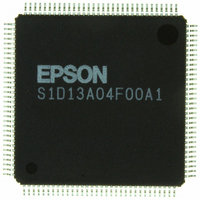
S1D13A04F00A Epson Electronics America Inc-Semiconductor Div, S1D13A04F00A Datasheet - Page 539

S1D13A04F00A
Manufacturer Part Number
S1D13A04F00A
Description
IC LCD COMPANION 160KB 128-TQFP
Manufacturer
Epson Electronics America Inc-Semiconductor Div
Specifications of S1D13A04F00A
Display Type
LCD
Voltage - Supply
1.8 V ~ 2.75 V
Mounting Type
Surface Mount
Package / Case
125-TQFP, 125-VQFP
Lead Free Status / RoHS Status
Lead free / RoHS Compliant
Current - Supply
-
Operating Temperature
-
Interface
-
Configuration
-
Digits Or Characters
-
Other names
S1D13A04F00A100
S1D13A04F00A100
S1D13A04F00A100
Available stocks
Company
Part Number
Manufacturer
Quantity
Price
Company:
Part Number:
S1D13A04F00A
Manufacturer:
Epson Electronics America Inc-Semiconductor Div
Quantity:
10 000
Company:
Part Number:
S1D13A04F00A1
Manufacturer:
EPSON
Quantity:
816
Part Number:
S1D13A04F00A1
Manufacturer:
EPSON/爱普生
Quantity:
20 000
Company:
Part Number:
S1D13A04F00A100
Manufacturer:
OSRAM
Quantity:
4 600
- Current page: 539 of 598
- Download datasheet (6Mb)
Epson Research and Development
Vancouver Design Center
4.3 Register/Memory Mapping
4.4 MCF5307 Chip Select Configuration
Interfacing to the Motorola MCF5307 "ColdFire" Microprocessor
Issue Date: 01/10/12
Note
The S1D13A04 uses two 256K byte blocks which are selected using A18 from the
MCF5307 (A18 is connected to the S1D13A04 M/R# pin). The internal registers occupy
the first 256K bytes block and the 160K byte display buffer occupies the second 256K byte
block. These two blocks of memory are aliased over the entire 2M byte space.
Chip Selects 0 and 1 have programmable block sizes from 64K bytes through 2G bytes.
However, these chip selects would normally be needed to control system RAM and ROM.
Therefore, one of the IO chip selects CS2 through CS7 is required to address the entire
address space of the S1D13A04. These IO chip selects have a fixed, 2M byte block size. In
the example interface, chip select 4 is used to control the S1D13A04. The CSBAR register
should be set to the upper 8 bits of the desired base address.
The following options should be selected in the chip select mask registers (CSMR4/5).
• WP = 0 – disable write protect
• AM = 0 - enable alternate bus master access to the S1D13A04
• C/I = 1 - disable CPU space access to the S1D13A04
• SC = 1 - disable Supervisor Code space access to the S1D13A04
• SD = 0 - enable Supervisor Data space access to the S1D13A04
• UC = 1 - disable User Code space access to the S1D13A04
• UD = 0 - enable User Data space access to the S1D13A04
• V = 1 - global enable (“Valid”) for the chip select
The following options should be selected in the chip select control registers (CSCR4/5).
• WS0-3 = 0 - no internal wait state setting
• AA = 0 - no automatic acknowledgment
• PS (1:0) = 1:0 – memory port size is 16 bits
• BEM = 0 – Byte enable/write enable active on writes only
• BSTR = 0 – disable burst reads
• BSTW = 0 – disable burst writes
If aliasing is not desirable, the upper addresses must be fully decoded.
X37A-G-010-01
S1D13A04
Page 15
Related parts for S1D13A04F00A
Image
Part Number
Description
Manufacturer
Datasheet
Request
R

Part Number:
Description:
IC CONTROLLER CRT/LCD/TV 128-QFP
Manufacturer:
Epson Electronics America Inc-Semiconductor Div
Part Number:
Description:
IC GRAPHIC LCD CTRLR 256-PBGA
Manufacturer:
Epson Electronics America Inc-Semiconductor Div
Datasheet:
Part Number:
Description:
MEMORY CARD 2M STATIC RAM
Manufacturer:
Epson Electronics America Inc-Semiconductor Div
Part Number:
Description:
IC CTRLR/PHY USB OTG 64-QFP
Manufacturer:
Epson Electronics America Inc-Semiconductor Div
Part Number:
Description:
IC CONTROLLER USB 2.0 64-QFP
Manufacturer:
Epson Electronics America Inc-Semiconductor Div

Part Number:
Description:
IC PHY CONT 2PORT 1394A 100-QFP
Manufacturer:
Epson Electronics America Inc-Semiconductor Div
Part Number:
Description:
IC LINK CTRLR 1394 IDE-33 184QFP
Manufacturer:
Epson Electronics America Inc-Semiconductor Div
Part Number:
Description:
IC LINK CTRLR 1394 IDE-66 184QFP
Manufacturer:
Epson Electronics America Inc-Semiconductor Div

Part Number:
Description:
IC LINK CTRLR 1394 IDE100 100QFP
Manufacturer:
Epson Electronics America Inc-Semiconductor Div

Part Number:
Description:
IC LINK CTRLR/PHY 1394 100-QFP
Manufacturer:
Epson Electronics America Inc-Semiconductor Div
Part Number:
Description:
IC CTRLR/PHY USB 2.0 64-QFP
Manufacturer:
Epson Electronics America Inc-Semiconductor Div

Part Number:
Description:
IC CTRLR/PHY USB 2.0 100-QFP
Manufacturer:
Epson Electronics America Inc-Semiconductor Div
Part Number:
Description:
IC CHARGE CTRLR LI-ION 24-SSOP
Manufacturer:
Epson Electronics America Inc-Semiconductor Div
Part Number:
Description:
IC BATTERY LEAK PREVENTION SOT89
Manufacturer:
Epson Electronics America Inc-Semiconductor Div
Part Number:
Description:
IC BATTERY LEAK PREVENTION SOT89
Manufacturer:
Epson Electronics America Inc-Semiconductor Div


