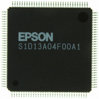
S1D13A04F00A Epson Electronics America Inc-Semiconductor Div, S1D13A04F00A Datasheet - Page 35

S1D13A04F00A
Manufacturer Part Number
S1D13A04F00A
Description
IC LCD COMPANION 160KB 128-TQFP
Manufacturer
Epson Electronics America Inc-Semiconductor Div
Specifications of S1D13A04F00A
Display Type
LCD
Voltage - Supply
1.8 V ~ 2.75 V
Mounting Type
Surface Mount
Package / Case
125-TQFP, 125-VQFP
Lead Free Status / RoHS Status
Lead free / RoHS Compliant
Current - Supply
-
Operating Temperature
-
Interface
-
Configuration
-
Digits Or Characters
-
Other names
S1D13A04F00A100
S1D13A04F00A100
S1D13A04F00A100
Available stocks
Company
Part Number
Manufacturer
Quantity
Price
Company:
Part Number:
S1D13A04F00A
Manufacturer:
Epson Electronics America Inc-Semiconductor Div
Quantity:
10 000
Company:
Part Number:
S1D13A04F00A1
Manufacturer:
EPSON
Quantity:
816
Part Number:
S1D13A04F00A1
Manufacturer:
EPSON/爱普生
Quantity:
20 000
Company:
Part Number:
S1D13A04F00A100
Manufacturer:
OSRAM
Quantity:
4 600
- Current page: 35 of 598
- Download datasheet (6Mb)
Epson Research and Development
Vancouver Design Center
4.3.3 Clock Input
4.3.4 Miscellaneous
4.3.5 Power And Ground
Hardware Functional Specification
Issue Date: 2003/05/01
COREVDD
Pin Name
Pin Name
Pin Name
USBCLK
CNF[6:0]
TESTEN
IOVDD
CLKI2
CLKI
VSS
Type
Type
Type
P
P
P
I
I
I
I
I
C9,C8,B8
F9,B10,K
,D7,C7,B
A10,F11
PFBGA
PFBGA
PFBGA
L10,J10
A2,C2,
K2,G5,
L2,G4,
H6,L9,
B2,F2,
Pin#
Pin#
Pin#
7,A7
F5
B9
E7
J8
10
1, 64-65,
TQFP15
TQFP15
TQFP15
102-108
20, 33,
46, 61,
18, 32,
45, 62,
79, 96,
80, 97
Pin#
Pin#
Pin#
109
128
127
19
99
59
Table 4-6: Power And Ground Pin Descriptions
Table 4-5: Miscellaneous Pin Descriptions
Table 4-4: Clock Input Pin Descriptions
Cell
Cell
Cell
T1
CI
CI
CI
LI
P
P
P
RESET#
RESET#
RESET#
State
State
State
Revision 6.0
—
—
—
—
—
—
—
—
Typically used as input clock source for bus clock and
memory clock
Typically used as input clock source for pixel clock
Typically used as input clock source for USB
These inputs are used to configure the S1D13A04 - see Table
4-7: “Summary of Power-On/Reset Options,” on page 30.
Note: These pins are used for configuration of the
S1D13A04 and must be connected directly to IO V
V
Test Enable input used for production test only (has type 1
pull-down resistor with a typical value of 50K
Note: This pin must not be connected.
6 IO V
2 double-bonded Core V
4 Core V
7 V
SS
SS
.
DD
pins.
DD.
pins.
pins on PFBGA package.
Description
Description
Description
DD.
pins on TQFP package.
at 3.3V).
X37A-A-001-06
S1D13A04
DD
Page 29
or
Related parts for S1D13A04F00A
Image
Part Number
Description
Manufacturer
Datasheet
Request
R

Part Number:
Description:
IC CONTROLLER CRT/LCD/TV 128-QFP
Manufacturer:
Epson Electronics America Inc-Semiconductor Div
Part Number:
Description:
IC GRAPHIC LCD CTRLR 256-PBGA
Manufacturer:
Epson Electronics America Inc-Semiconductor Div
Datasheet:
Part Number:
Description:
MEMORY CARD 2M STATIC RAM
Manufacturer:
Epson Electronics America Inc-Semiconductor Div
Part Number:
Description:
IC CTRLR/PHY USB OTG 64-QFP
Manufacturer:
Epson Electronics America Inc-Semiconductor Div
Part Number:
Description:
IC CONTROLLER USB 2.0 64-QFP
Manufacturer:
Epson Electronics America Inc-Semiconductor Div

Part Number:
Description:
IC PHY CONT 2PORT 1394A 100-QFP
Manufacturer:
Epson Electronics America Inc-Semiconductor Div
Part Number:
Description:
IC LINK CTRLR 1394 IDE-33 184QFP
Manufacturer:
Epson Electronics America Inc-Semiconductor Div
Part Number:
Description:
IC LINK CTRLR 1394 IDE-66 184QFP
Manufacturer:
Epson Electronics America Inc-Semiconductor Div

Part Number:
Description:
IC LINK CTRLR 1394 IDE100 100QFP
Manufacturer:
Epson Electronics America Inc-Semiconductor Div

Part Number:
Description:
IC LINK CTRLR/PHY 1394 100-QFP
Manufacturer:
Epson Electronics America Inc-Semiconductor Div
Part Number:
Description:
IC CTRLR/PHY USB 2.0 64-QFP
Manufacturer:
Epson Electronics America Inc-Semiconductor Div

Part Number:
Description:
IC CTRLR/PHY USB 2.0 100-QFP
Manufacturer:
Epson Electronics America Inc-Semiconductor Div
Part Number:
Description:
IC CHARGE CTRLR LI-ION 24-SSOP
Manufacturer:
Epson Electronics America Inc-Semiconductor Div
Part Number:
Description:
IC BATTERY LEAK PREVENTION SOT89
Manufacturer:
Epson Electronics America Inc-Semiconductor Div
Part Number:
Description:
IC BATTERY LEAK PREVENTION SOT89
Manufacturer:
Epson Electronics America Inc-Semiconductor Div


